|
|
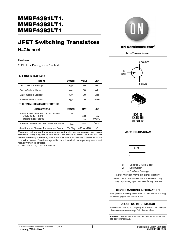
JFET Switching Transistors
www.DataSheet4U.com MMBF4391LT1, MMBF4392LT1, MMBF4393LT1 JFET Switching Transistors N−Channel http://onsemi.com Featur...
| @ 2014 :: Datasheetspdf.com :: Semiconductors datasheet search & download site. (Privacy Policy & Contact) |