MM74HCU04 Hex Inverter
September 1983 Revised February 1999
MM74HCU04 Hex Inverter
General Description
The MM74HCU04 i...
MM74HCU04 Hex Inverter
September 1983 Revised February 1999
MM74HCU04 Hex Inverter
General Description
The MM74HCU04 inverters utilize advanced silicon-gate
CMOS technology to achieve operating speeds similar to LS-TTL gates with the low power consumption of standard
CMOS integrated circuits. The MM74HCU04 is an unbuffered inverter. It has high noise immunity and the ability to drive 15 LS-TTL loads. The 74HCU logic family is functionally as well as pin-out compatible with the standard 74LS logic family. All inputs are protected from damage due to static discharge by internal diode clamps to VCC and ground.
Features
s Typical propagation delay: 7 ns s Fanout of 15 LS-TTL loads s Quiescent power consumption: 10 µA maximum at room temperature s Low input current: 1 µA maximum
Ordering Code:
Order Number MM74HCU04M MM74HCU04SJ MM74HCU04MTC MM74HCU04N Package Number M14A M14D MTC14 N14A Package Description 14-Lead Small Outline Integrated Circuit (SOIC), JEDEC MS-120, 0.150” Narrow 14-Lead Small Outline Package (SOP), EIAJ TYPE II, 5.3mm Wide 14-Lead Thin Shrink Small Outline Package (TSSOP), JEDEC MO-153, 4.4mm Wide 14-Lead Plastic Dual-In-Lead Package (PDIP), JEDEC MS-001, 0.300” Wide
Devices also available in Tape and Reel. Specify by appending the suffix letter “X” to the ordering code.
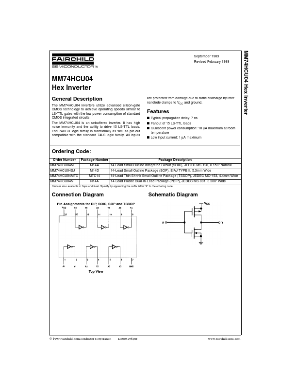
Connection Diagram
Pin Assignments for DIP, SOIC, SOP and TSSOP
Schematic Diagram
Top View
© 1999 Fairchild Semiconductor Corporation
DS005296.prf
www.fairchildsemi.com
MM74HCU04
...