MM74HC259 8-Bit Addressable Latch/3-to-8 Line Decoder
September 1983 Revised February 1999
MM74HC259 8-Bit Addressable...
MM74HC259 8-Bit Addressable Latch/3-to-8 Line Decoder
September 1983 Revised February 1999
MM74HC259 8-Bit Addressable Latch/3-to-8 Line Decoder
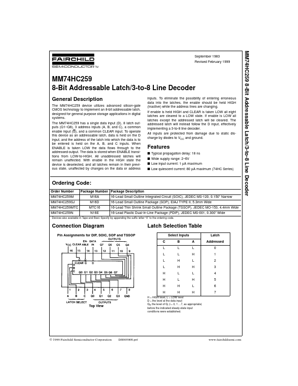
General Description
The MM74HC259 device utilizes advanced silicon-gate
CMOS technology to implement an 8-bit addressable latch, designed for general purpose storage applications in digital systems. The MM74HC259 has a single data input (D), 8 latch outputs (Q1–Q8), 3 address inputs (A, B, and C), a common enable input (G), and a common CLEAR input. To operate this device as an addressable latch, data is held on the D input, and the address of the latch into which the data is to be entered is held on the A, B, and C inputs. When ENABLE is taken LOW the data flows through to the addressed output. The data is stored when ENABLE transitions from LOW-to-HIGH. All unaddressed latches will remain unaffected. With enable in the HIGH state the device is deselected, and all latches remain in their previous state, unaffected by changes on the data or address inputs. To eliminate the possibility of entering erroneous data into the latches, the enable should be held HIGH (inactive) while the address lines are changing. If enable is held HIGH and CLEAR is taken LOW all eight latches are cleared to a LOW state. If enable is LOW all latches except the addressed latch will be cleared. The addressed latch will instead follow the D input, effectively implementing a 3-to-8 line decoder. All inputs are protected from damage due to static discharge by ...