MM74HC00 — Quad 2-Input NAND Gate
February 2008
MM74HC00 Quad 2-Input NAND Gate
Features
■ Typical propagation delay:...
MM74HC00 — Quad 2-Input NAND Gate
February 2008
MM74HC00 Quad 2-Input NAND Gate
Features
■ Typical propagation delay: 8ns ■ Wide power supply range: 2V–6V ■ Low quiescent current: 20µA maximum (74HC Series) ■ Low input current: 1µA maximum ■ Fanout of 10 LS-TTL loads
General Description
The MM74HC00 NAND gates utilize advanced silicongate
CMOS technology to achieve operating speeds similar to LS-TTL gates with the low power consumption of standard
CMOS integrated circuits. All gates have buffered outputs. All devices have high noise immunity and the ability to drive 10 LS-TTL loads. The 74HC logic family is functionally as well as pin-out compatible with the standard 74LS logic family. All inputs are protected from damage due to static discharge by internal diode clamps to VCC and ground.
Ordering Information
Package Order Number Number
Package Description
MM74HC00M MM74HC00SJ MM74HC00MTC
M14A M14D MTC14
14-Lead Small Outline Integrated Circuit (SOIC), JEDEC MS-012, 0.150" Narrow 14-Lead Small Outline Package (SOP), EIAJ TYPE II, 5.3mm Wide 14-Lead Thin Shrink Small Outline Package (TSSOP), JEDEC MO-153, 4.4mm Wide
MM74HC00N
N14A 14-Lead Plastic 
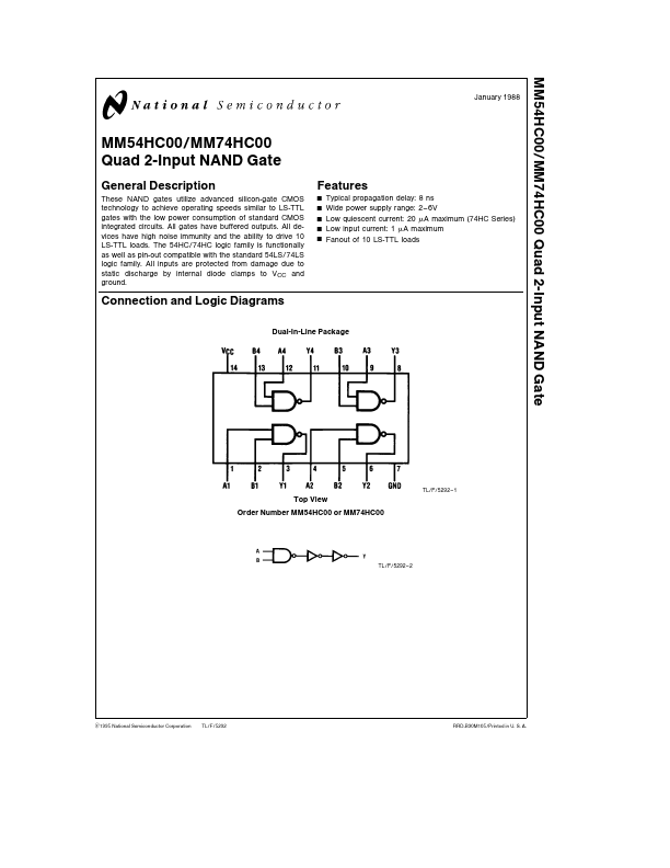
Dual-In-Line Package (PDIP), JEDEC MS-001, 0.300" Wide
Device also available in Tape and Reel. Specify by appending suffix letter “X” to the ordering number.
All packages are lead free per JEDEC: J-STD-020B standard.
Connection Diagram
Pin Assignments for DIP, SOIC, SOP and TSSOP
Logic Diagram
Top View
©1983 Fairchild...