MM74C165 Parallel-Load 8-Bit Shift Register
October 1987 Revised January 1999
MM74C165 Parallel-Load 8-Bit Shift Regis...
MM74C165 Parallel-Load 8-Bit Shift Register
October 1987 Revised January 1999
MM74C165 Parallel-Load 8-Bit Shift Register
General Description
The MM74C165 functions as an 8-bit parallel-load, serial shift register. Data is loaded into the register independent of the state of the clock(s) when PARALLEL LOAD (PL) is low. Shifting is inhibited as long as PL is low. Data is sequentially shifted from complementary outputs, Q7 and Q7, highest-order bit (P7) first. New serial data may be entered via the SERIAL DATA (Ds) input. Serial shifting occurs on the rising edge of CLOCK1 or CLOCK2. Clock inputs may be used separately or together for combined clocking from independent sources. Either clock input may be used also as an active-low clock enable. To prevent double-clocking when a clock input is used as an enable, the enable must be changed to a high level (disabled) only while the clock is HIGH.
Features
s Wide supply
voltage range: s Guaranteed noise margin: s High noise immunity: 3V to 15V 1V fan out of 2 driving 74L 0.45 VCC (typ.)
s Low power TTL compatibility: s Dual clock inputs s Fully static operation
s Parallel loading independent of clock
Ordering Code:
Order Number MM74165N Package Number N16E Package Description 16-Lead Plastic Dual-In-Line Package (PDIP), JEDEC MS-001, 0.300” Wide
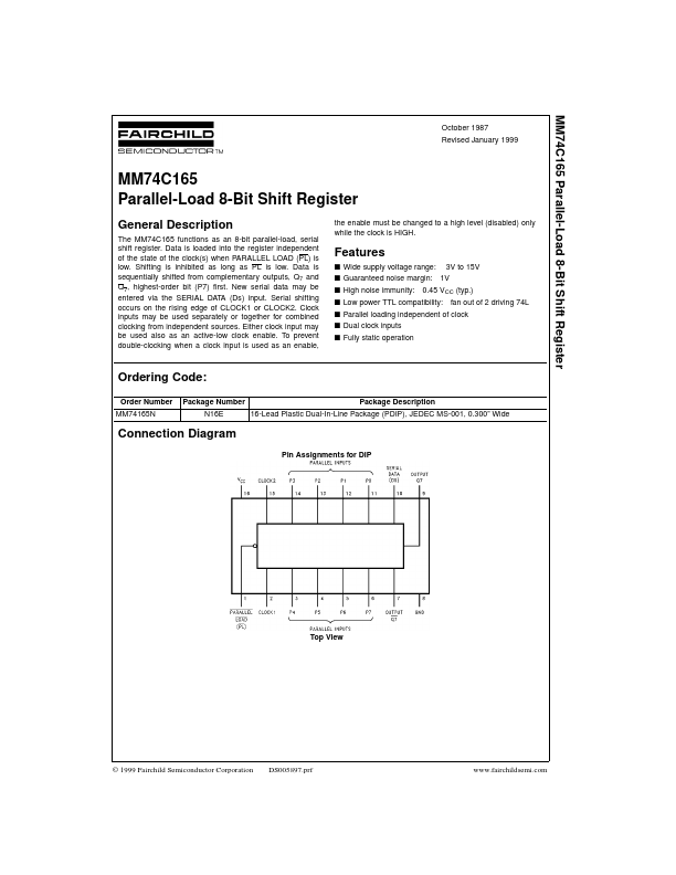
Connection Diagram
Pin Assignments for DIP
Top View
© 1999 Fairchild Semiconductor Corporation
DS005897.prf
www.fairchildsemi.com
MM74C165
Block Diagrams
*Please look into Sect...