3.3 V Communications Clock PLL
MK2049-35 3.3 V Communications Clock PLL
Description
The MK2049-35 is a Phase-Locked Loop (PLL) based clock synthesizer ...
Description
MK2049-35 3.3 V Communications Clock PLL
Description
The MK2049-35 is a Phase-Locked Loop (PLL) based clock synthesizer that accepts multiple input frequencies. With an 8 kHz clock input as a reference, the MK2049-35 generates T1, E1, T3, E3, OC3/3, Gigabit Ethernet, and other communications frequencies. This allows for the generation of clocks frequency-locked to an 8 kHz backplane clock, simplifying clock synchronization in communications systems. This part also has a jitter-attenuated Buffer capability. In this mode, the MK2049-35 is ideal for filtering jitter from with high jitter clocks. ICS/MicroClock can customize these devices for many other different frequencies. Contact your ICS/MicroClock representative for more details.
Features
Packaged in 20 pin SOIC 3.3 V ±5% operation Meets the TR62411, ETS300 011, and GR-1244 specification for MTIE, Pull-in/Hold-in Range, Phase Transients, and Jitter Generation for Stratum 3, 4, and 4E Accepts multiple inputs: 8 kHz backplane clock, or 10 to 50 MHz Locks to 8 kHz ±100 ppm (External mode) Buffer Mode allows jitter attenuation of 10-50 MHz input and x1/x0.5 or x1/x2 outputs Exact internal ratios enable zero ppm error Output clock rates include T1, E1, T3, E3, and OC3 submultiples See the MK2049-01, -02, and -03 for more selections at VDD = 5 V, and the MK2049-34 for more selections at 3.3 V GND 3 RES
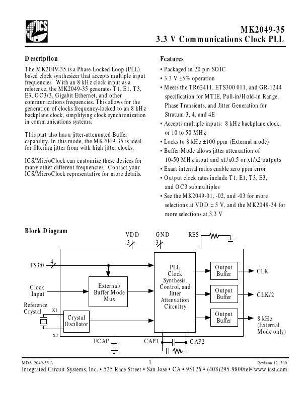
Block Diagram
VDD 3
FS3:0
4
Clock Input Reference X1 Crystal Crystal Oscillator
X2
External/ Buffer Mode...
Similar Datasheet