www.DataSheet4U.com
MJD200 (NPN) MJD210 (PNP) Complementary Plastic Power Transistors
NPN/PNP Silicon DPAK For Surface ...
www.DataSheet4U.com
MJD200 (NPN) MJD210 (PNP) Complementary Plastic Power Transistors
NPN/PNP Silicon DPAK For Surface Mount Applications
Designed for low
voltage, low−power, high−gain audio amplifier applications.
Features http://onsemi.com
Collector−Emitter Sustaining
Voltage − High DC Current Gain − hFE = 70 (Min) @ IC = 500 mAdc
= 45 (Min) @ IC = 2 Adc = 10 (Min) @ IC = 5 Adc Lead Formed for Surface Mount Applications in Plastic Sleeves (No Suffix) Low Collector−Emitter Saturation
Voltage − VCE(sat) = 0.3 Vdc (Max) @ IC = 500 mAdc = 0.75 Vdc (Max) @ IC = 2.0 Adc High Current−Gain − Bandwidth Product − fT = 65 MHz (Min) @ IC = 100 mAdc Annular Construction for Low Leakage − ICBO = 100 nAdc @ Rated VCB Epoxy Meets UL 94 V−0 @ 0.125 in ESD Ratings: Human Body Model, 3B u 8000 V Machine Model, C u 400 V Pb−Free Packages are Available VCEO(sus) = 25 Vdc (Min) @ IC = 10 mAdc
SILICON POWER TRANSISTORS 5 AMPERES 25 VOLTS, 12.5 WATTS
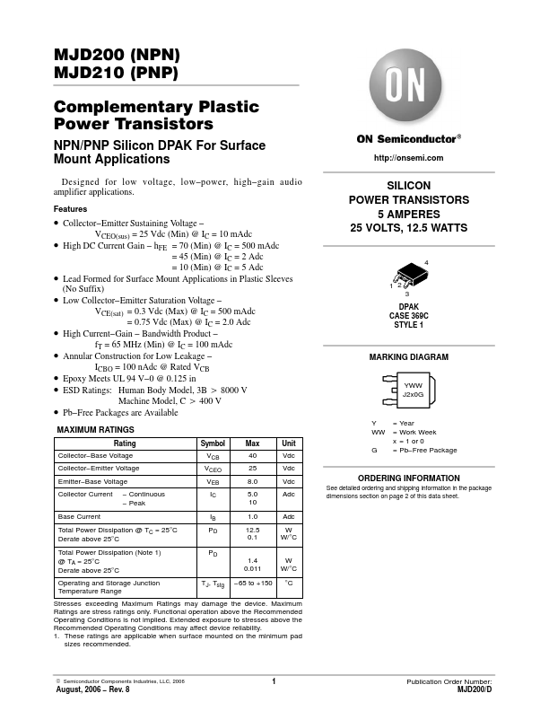
4 1 2 3 DPAK CASE 369C STYLE 1
MARKING DIAGRAM
YWW J2x0G
MAXIMUM RATINGS
Rating Collector−Base
Voltage Collector−Emitter
Voltage Emitter−Base
Voltage Collector Current Base Current Total Power Dissipation @ TC = 25°C Derate above 25°C Total Power Dissipation (Note 1) @ TA = 25°C Derate above 25°C Operating and Storage Junction Temperature Range − Continuous − Peak Symbol VCB VCEO VEB IC IB PD PD 1.4 0.011 TJ, Tstg −65 to +150 W W/°C °C Max 40 25 8.0 5.0 10 1.0 12.5 0.1 Unit Vdc Vdc Vdc Adc Adc W W/°C
Y WW G
= = x =
Year Work...