MITSUBISHI SEMICONDUCTOR 〈GaAs FET〉
MGF0911A
L, S BAND POWER GaAs FET
DESCRIPTION
The MGF0911A, GaAs FET with an N-cha...
MITSUBISHI SEMICONDUCTOR 〈GaAs FET〉
MGF0911A
L, S BAND POWER GaAs FET
DESCRIPTION
The MGF0911A, GaAs FET with an N-channel schottky gate, is designed for use in UHF band
amplifiers.
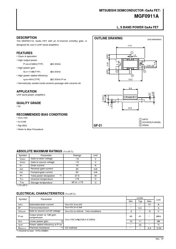
OUTLINE DRAWING
17.5
1
Unit:millimeters
FEATURES
Class A operation High output power P1dB=41dBm(TYP) High power gain GLP=11dB(TYP) High power added efficiency ηadd=40%(TYP) @2.3GHz,P1dB Hermetically sealed metal-ceramic package with ceramic lid @2.3GHz
2
1.0
@2.3GHz
2 3
2-R1.25
14.3
9.4
APPLICATION
UHF band power
amplifiers
QUALITY GRADE
IG
10.0
RECOMMENDED BIAS CONDITIONS
VDS=10V ID=2.6A Rg=50Ω Refer to Bias Procedure
1 GATE 2 SOURCE(FLANGE)
GF-21
3 DRAIN
ABSOLUTE MAXIMUM RATINGS (Ta=25˚C)
Symbol VGDO VGSO ID IGR IGF PT Tch Tstg
*1:TC=25˚C
Parameter Gate to drain
voltage Gate to source
voltage Drain current Reverse gate current Forward gate current Total power dissipation Channel temperature Storage temperature
Ratings -15 -15 10 30 63 37.5 175 -65 to +175
*1
Unit V V A mA mA W ˚C ˚C
ELECTRICAL CHARACTERISTICS (Ta=25˚C)
Symbol IDSS gm VGS(off) P1dB GLP ηadd Rth(ch-c) Parameter Saturated drain current Transconductance Gate to source cut-off
voltage Output power at 1dB gain compression VDS=3V,VGS=0V VDS=3V,ID=2.6A VDS=3V,ID=20mA Test conditions Min – – -2 40 VDS=10V,ID 2.6A,f=2.3GHz 10 – – Limits Typ – 3.0 – 41 11 40 – Max 10 – -5 – – – 4.0 Unit A S V dBm dB % ˚C/W
Linear power gain *2 Power added efficiency at P1dB Thermal resistance *1 ∆Vf method
*1:Chan...