MC74LVX125
Quad Bus Buffer
With 5 V−Tolerant Inputs
The MC74LVX125 is an advanced high speed CMOS quad bus buffer. The...
MC74LVX125
Quad Bus Buffer
With 5 V−Tolerant Inputs
The MC74LVX125 is an advanced high speed
CMOS quad bus buffer. The inputs tolerate
voltages up to 7.0 V, allowing the interface of 5.0 V systems to 3.0 V systems.
The MC74LVX125 requires the 3−state control input (OE) to be set High to place the output into the high impedance state.
Features
High Speed: tPD = 4.4 ns (Typ) at VCC = 3.3 V Low Power Dissipation: ICC = 4 mA (Max) at TA = 25°C Power Down Protection Provided on Inputs Balanced Propagation Delays Low Noise: VOLP = 0.5 V (Max) Pin and Function Compatible with Other Standard Logic Families Latchup Performance Exceeds 300 mA ESD Performance: Human Body Model > 2000 V
Machine Model > 200 V
These Devices are Pb−Free and are RoHS Compliant
1 OE0
2 D0
4 OE1
5 D1
3 O0
6 O1
10 OE2
9 D2
13 OE3
12 D3
8 O2
11 O3
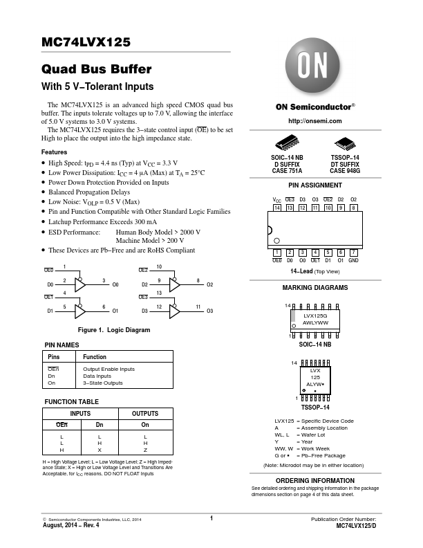
Figure 1. Logic Diagram
PIN NAMES
Pins
Function
OEn Dn On
Output Enable Inputs Data Inputs 3−State Outputs
FUNCTION TABLE
INPUTS
OEn
Dn
OUTPUTS On
LL LH HX
L H Z
H = High
Voltage Level; L = Low
Voltage Level; Z = High Impedance State; X = High or Low
Voltage Level and Transitions Are Acceptable, for ICC reasons, DO NOT FLOAT Inputs
http://onsemi.com
SOIC−14 NB D SUFFIX CASE 751A
TSSOP−14 DT SUFFIX CASE 948G
PIN ASSIGNMENT
VCC OE3 D3 O3 OE2 D2 O2 14 13 12 11 10 9 8
1234567 OE0 D0 O0 OE1 D1 O1 GND
14−Lead (Top View)
MARKING DIAGRAMS
14
LVX125G AWLYWW
1 SOIC−14 NB
14 LVX 125
ALYWG G
1 TSSOP−14
LVX125 = Specific Device Code A = A...