MC74AC20, MC74ACT20
Dual 4-Input NAND Gate
High−Performance Silicon−Gate CMOS
Features
• Outputs Source/Sink 24 mA • ′AC...
MC74AC20, MC74ACT20
Dual 4-Input NAND Gate
High−Performance Silicon−Gate
CMOS
Features
Outputs Source/Sink 24 mA ′ACT20 Has TTL Compatible Inputs These are Pb−Free Devices
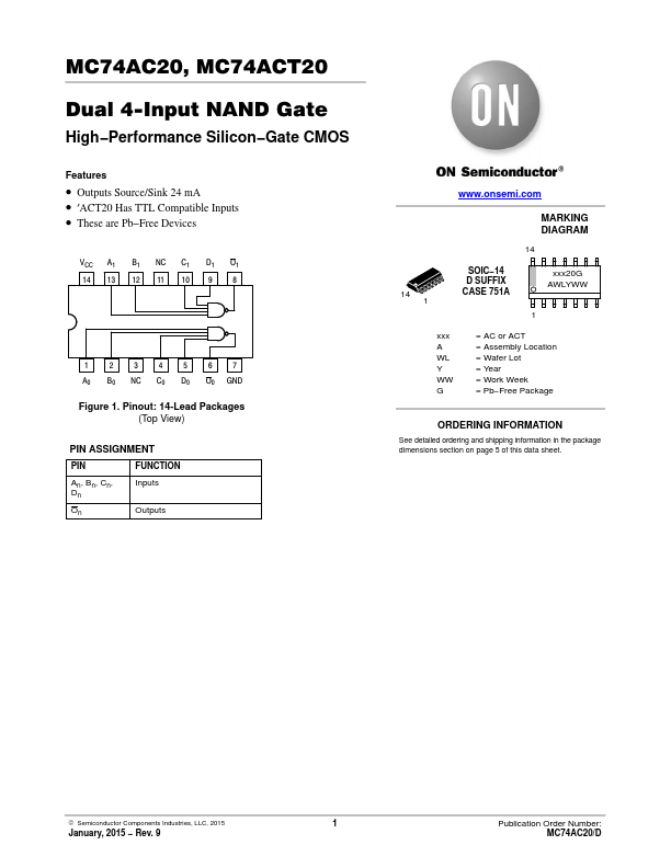
VCC A1 B1 NC C1 D1 O1 14 13 12 11 10 9 8
1234567 A0 B0 NC C0 D0 O0 GND
Figure 1. Pinout: 14-Lead Packages (Top View)
PIN ASSIGNMENT
PIN FUNCTION
An, Bn, Cn, Dn
On
Inputs Outputs
www.onsemi.com
MARKING DIAGRAM
14
14 1
SOIC−14 D SUFFIX CASE 751A
xxx20G AWLYWW
1
xxx = AC or ACT A = Assembly Location WL = Wafer Lot Y = Year WW = Work Week G = Pb−Free Package
ORDERING INFORMATION
See detailed ordering and shipping information in the package dimensions section on page 5 of this data sheet.
© Semiconductor Components Industries, LLC, 2015
January, 2015 − Rev. 9
1
Publication Order Number: MC74AC20/D
MC74AC20, MC74ACT20
MAXIMUM RATINGS
Symbol
Parameter
Value
Unit
VCC VI VO IIK IOK IO ICC IGND TSTG TL TJ qJA PD MSL
DC Supply
Voltage DC Input
Voltage DC Output
Voltage DC Input Diode Current DC Output Diode Current DC Output Sink/Source Current DC Supply Current per Output Pin DC Ground Current per Output Pin Storage Temperature Range Lead temperature, 1 mm from Case for 10 Seconds Junction temperature under Bias Thermal Resistance (Note 2) Power Dissipation in Still Air at 85°C Moisture Sensitivity
(Note 1)
*0.5 to )7.0 *0.5 v VI v VCC )0.5 *0.5 v VO v VCC )0.5
$20 $50 $50 $50 $50 *65 to )150 260 )150 125 125 Level 1
V V V mA mA mA mA mA °C °C °C °C/W mW
FR VESD
Flammability Rating E...