Dual 2-Wide 2-3-Input OR-AND/OR-AND Gate
MC10117 Dual 2-Wide 2-3-Input OR-AND/OR-AND Gate
T h e M C 1 0 11 7 i s a d u a l 2 – w i d e 2 – 3 – i n p u t OR–AND/O...
Description
MC10117 Dual 2-Wide 2-3-Input OR-AND/OR-AND Gate
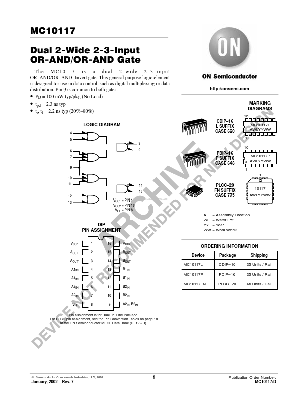
T h e M C 1 0 11 7 i s a d u a l 2 – w i d e 2 – 3 – i n p u t OR–AND/OR–AND–Invert gate. This general purpose logic element is designed for use in data control, such as digital multiplexing or data distribution. Pin 9 is common to both gates. PD = 100 mW typ/pkg (No Load) tpd = 2.3 ns typ tr, tf = 2.2 ns typ (20%–80%)
LOGIC DIAGRAM
4 5 6 7 9 10 11 12 13 14 15 VCC1 = PIN 1 VCC2 = PIN 16 VEE = PIN 8
www.DataSheet4U.com
http://onsemi.com MARKING DIAGRAMS
16 CDIP–16 L SUFFIX CASE 620 1 MC10117L AWLYYWW
3 2 PDIP–16 P SUFFIX CASE 648
16 MC10117P AWLYYWW 1 1 PLCC–20 FN SUFFIX CASE 775 10117 AWLYYWW
DIP PIN ASSIGNMENT
VCC1 AOUT AOUT A1IN A1IN A2IN A2IN VEE 1 2 3 4 5 6 7 8 16 15 14 13 12 11 10 9 VCC2 BOUT BOUT B1IN B1IN B2IN B2IN A2IN, B2IN MC10117P
A WL YY WW
= Assembly Location = Wafer Lot = Year = Work Week
ORDERING INFORMATION
Device MC10117L Package CDIP–16 PDIP–16 PLCC–20 Shipping 25 Units / Rail 25 Units / Rail 46 Units / Rail
MC10117FN
Pin assignment is for Dual–in–Line Package. For PLCC pin assignment, see the Pin Conversion Tables on page 18 of the ON Semiconductor MECL Data Book (DL122/D).
© Semiconductor Components Industries, LLC, 2002
1
January, 2002 – Rev. 7
Publication Order Number: MC10117/D
MC10117
ELECTRICAL CHARACTERISTICS
Test Limits Pin Under Test 8 6 9 4 4 2 3 2 3 2 3 2 3 0.5 –1.060 –1.060 –1.890 –1.890 –1.080 –1.080 –1.655 –1.655 –0.890 –0.780 –1.675 –1.675 –30°C Min Max 29 425 560 390 0.5 –0...
Similar Datasheet