M54/M74HC365 M54/M74HC366
HEX BUS BUFFER (3-STATE) HC365 NON INVERTING - HC366 INVERTING
. . . . . . . .
HIGH SPEED tP...
M54/M74HC365 M54/M74HC366
HEX BUS BUFFER (3-STATE) HC365 NON INVERTING - HC366 INVERTING
. . . . . . . .
HIGH SPEED tPD = 9 ns (TYP) AT VCC = 5 V LOW POWER DISSIPATION ICC = 4 µA (MAX.) AT TA = 25 °C HIGH NOISE IMMUNITY VNIH = VNIL = 28 % VCC (MIN.) OUTPUT DRIVE CAPABILITY 15 LSTTL LOADS SYMMETRICAL OUTPUT IMPEDANCE |IOH| = IOL = 6 mA (MIN.) BALANCED PROPAGATION DELAYS tPLH = tPHL WIDE OPERATING
VOLTAGE RANGE VCC (OPR) = 2 V TO 6 V PIN AND FUNCTION COMPATIBLE WITH 54/74LS365/366
B1R (Plastic Package)
F1R (Ceramic Package)
M1R (Micro Package)
C1R (Chip Carrier)
ORDER CODES : M54HCXXXF1R M74HCXXXM1R M74HCXXXB1R M74HCXXXC1R
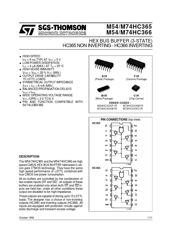
PIN CONNECTIONS (top view)
HC365
DESCRIPTION The M54/74HC365 and the M54/74HC366 are high speed
CMOS HEX BUS BUFFER fabricated in sili2 con gate C MOS technology. They have the same high speed performance of LSTTL combined with true
CMOS low power consumption. All six buffers are controlled by the combination of two enable inputs (G1 and G2) ; all outputs of these buffers are enabled only when both G1 and G2 inputs are held low, under all other conditions these output are disabled to be high-impedance. These outputs are capable of driving up to 15 LSTTL loads. The designer has a choice of non-inverting outputs (HC365) and inverting outputs (HC366). All inputs are equipped with protection circuits against static discharge and transient excess
voltage.
October 1992 1/11
HC366
M54/M74HC365/366
INPUT AND OUTPUT EQUIVALENT CIRCUIT
CHIP CARRIER HC365 HC...