M54HC173 M74HC173
QUAD D-TYPE REGISTER (3-STATE)
. . . . . . . .
HIGH SPEED fMAX = 73 MHz (TYP.) at VCC = 5 V LOW POWE...
M54HC173 M74HC173
QUAD D-TYPE REGISTER (3-STATE)
. . . . . . . .
HIGH SPEED fMAX = 73 MHz (TYP.) at VCC = 5 V LOW POWER DISSIPATION ICC = 4 µA (MAX.) at TA = 25 °C HIGH NOISE IMMUNITY VNIH = VNIL = 28 % VCC (MIN.) OUTPUT DRIVE CAPABILITY 15 LSTTL LOADS SYMMETRICAL OUTPUT IMPEDANCE |IOH| = IOL = 6 mA (MIN.) BALANCED PROPAGATION DELAYS tPLH = tPHL WIDE OPERATING
VOLTAGE RANGE VCC (OPR) = 2 V to 6 V PIN AND FUNCTION COMPATIBLE WITH 54/74LS 173
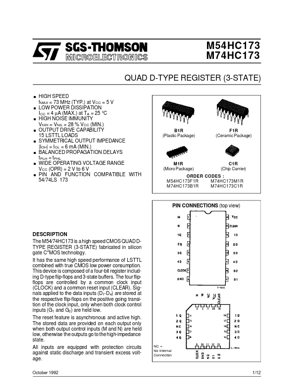
B1R (Plastic Package)
F1R (Ceramic Package)
M1R (Micro Package)
C1R (Chip Carrier)
ORDER CODES : M54HC173F1R M74HC173M1R M74HC173B1R M74HC173C1R
PIN CONNECTIONS (top view)
DESCRIPTION The M54/74HC173 is a high speed
CMOS QUAD DTYPE REGISTER (3-STATE) fabricated in silicon gate C2MOS technology. It has the same high speed performance of LSTTL combined with true
CMOS low power consumption. This device is composed of a four-bit register including D-type flip-flops and 3-state buffers. The four flipflops are controlled by a common clock input (CLOCK) and a common reset input (CLEAR). Signals applied to the data inputs (D1-D4) are stored at the respective flip-flops on the positive going transition of the clock input, only when both clock control inputs (G1 and G2) are held low. The reset feature is asynchronous and active high. The stored data are provided on each output only when both output control inputs (M and N) are held low, otherwise the outputs go to the high-impedance state. All inputs are equipped with protection circuits ag...