®
74ACT02
QUAD 2-INPUT NOR GATE
s s
s
s
s
s
s
s
s
HIGH SPEED: tPD = 5 ns (TYP.) at VCC = 5V LOW POWER DISSIPAT...
®
74ACT02
QUAD 2-INPUT NOR GATE
s s
s
s
s
s
s
s
s
HIGH SPEED: tPD = 5 ns (TYP.) at VCC = 5V LOW POWER DISSIPATION: ICC = 4 µA (MAX.) at TA = 25 oC COMPATIBLE WITH TTL OUTPUTS VIH = 2V (MIN), VIL = 0.8V (MAX) 50Ω TRANSMISSION LINE DRIVING CAPABILITY SYMMETRICAL OUTPUT IMPEDANCE: |IOH| = IOL = 24 mA (MIN) BALANCED PROPAGATION DELAYS: tPLH ≅ tPHL OPERATING
VOLTAGE RANGE: VCC (OPR) = 4.5V to 5.5V PIN AND FUNCTION COMPATIBLE WITH 74 SERIES 02 IMPROVED LATCH-UP IMMUNITY
DIP
PACKAGE DIP SOP TSSOP
SOP
ORDER CODES T UBE M74ACT02B M74ACT02M
TSSOP
T& R M74ACT02MTR M74ACT02TTR
DESCRIPTION The ACT02 is an advanced high-speed
CMOS QUAD 2-INPUT NOR GATE fabricated with sub-micron silicon gate and double-layer metal wiring C2MOS technology. It is ideal for low power applications mantaining high speed operation similar to equivalent Bipolar Schottky TTL.
The internal circuit is composed of 3 stages including buffer output, which enables high noise immunity and stable output. The device is designed to interface directly High Speed
CMOS systems with TTL, NMOS and
CMOS output
voltage levels. All inputs and outputs are equipped with protection circuits against static discharge, giving them 2KV ESD immunity and transient excess
voltage.
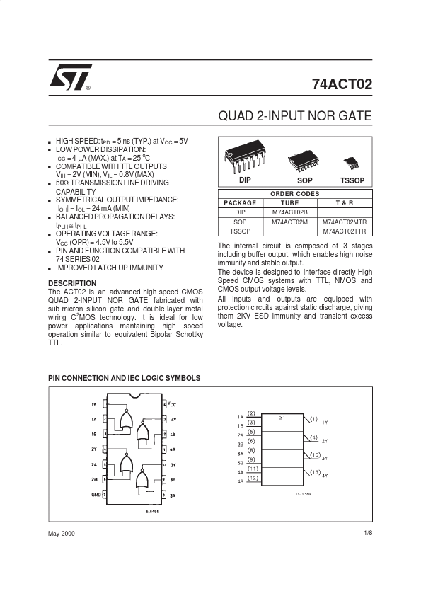
PIN CONNECTION AND IEC LOGIC SYMBOLS
May 2000
1/8
74ACT02
INPUT AND OUTPUT EQUIVALENT CIRCUIT PIN DESCRIPTION
PIN No 2, 5, 8, 11 3, 6, 9, 12 1, 4, 10, 12 7 14 SYMBOL 1A to 4A 1B to 4B 1Y to 4Y GND VCC NAME AND FUNCT ION Data Inputs Data Inputs Da...