MITSUBISHI (Dig./Ana. INTERFACE)
M62230FP
LCD MATRIX REGULATOR DESCRIPTION
The M62230FP is a semiconductor circuit for ...
MITSUBISHI (Dig./Ana. INTERFACE)
M62230FP
LCD MATRIX REGULATOR DESCRIPTION
The M62230FP is a semiconductor circuit for LCD matrix regulator, which will generate the diveded-
voltage to drive LCD matrix. By changing the connection of R pin(i.e.,Change the internal resistor ratio), M62230FP can support divided
voltage ratio ranging from 1/5 bias to 1/13 bias. The high stability and any desired
voltage levels is possible, since the variable
voltage regulator for Vref is built-in.
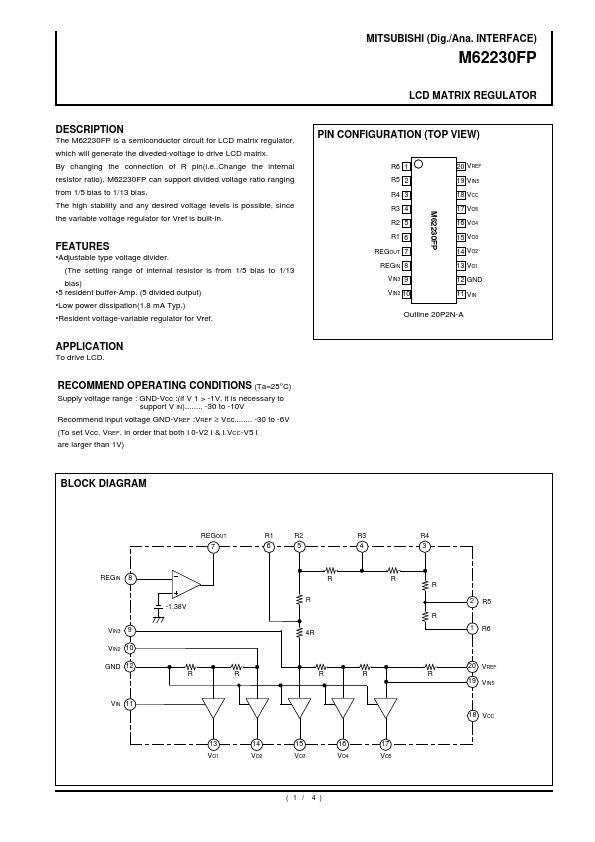
R6 1 R5 2 R4 3 R3 4 R2 5 R1 6 20 VREF 19 VIN5 18 VCC 17 VO5 16 VO4 15 VO3 14 VO2 13 VO1 12 GND 11 VIN
PIN CONFIGURATION (TOP VIEW)
FEATURES
Adjustable type
voltage divider. (The setting range of internal resistor is from 1/5 bias to 1/13 bias) 5 resident buffer-Amp. (5 divided output) Low power dissipation(1.8 mA Typ.) Resident
voltage-variable regulator for Vref.
REGOUT 7 REGIN 8 VIN3 9 VIN2 10
Outline 20P2N-A
APPLICATION
To drive LCD.
RECOMMEND OPERATING CONDITIONS (Ta=25°C)
Supply
voltage range : GND-Vcc :(if V 1 > -1V, it is necessary to support V IN)........ -30 to -10V Recommend input
voltage GND-VREF :VREF ≥ Vcc........ -30 to -6V (To set Vcc, VREF, in order that both I 0-V2 I & I VCC-V5 I are larger than 1V)
BLOCK DIAGRAM
REGOUT 7
R1 6
R2 5
R3 4
R4 3
REGIN
8 R -1.38V
R
R R 2 R R5
VIN3
9
4R
1
R6
VIN2 10 GND 12 R R R R R 19 VIN5 VIN 11 18 VCC 20 VREF
13 VO1
14 VO2
15 VO3
16 VO4
17 VO5
( 1 /
4 )
MITSUBISHI (Dig./Ana. INTERFACE)
M62230FP
LCD MATRIX REGULATOR
EXPLA...