M58WR064ET M58WR064EB
64 Mbit (4Mb x 16, Multiple Bank, Burst) 1.8V Supply Flash Memory
FEATURES SUMMARY s SUPPLY VOLTAG...
M58WR064ET M58WR064EB
64 Mbit (4Mb x 16, Multiple Bank, Burst) 1.8V Supply Flash Memory
FEATURES SUMMARY s SUPPLY
VOLTAGE – VDD = 1.65V to 2.2V for Program, Erase and Read – VDDQ = 1.65V to 3.3V for I/O Buffers – VPP = 12V for fast Program (optional)
s
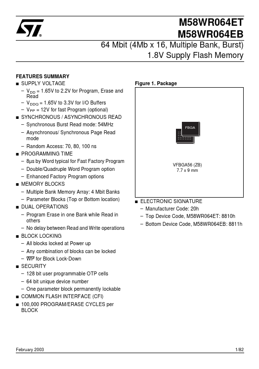
Figure 1. Package
SYNCHRONOUS / ASYNCHRONOUS READ – Synchronous Burst Read mode: 54MHz – Asynchronous/ Synchronous Page Read mode – Random Access: 70, 80, 100 ns
FBGA
s
PROGRAMMING TIME – 8µs by Word typical for Fast Factory Program – Double/Quadruple Word Program option – Enhanced Factory Program options
VFBGA56 (ZB) 7.7 x 9 mm
s
MEMORY BLOCKS – Multiple Bank Memory Array: 4 Mbit Banks – Parameter Blocks (Top or Bottom location)
s
ELECTRONIC SIGNATURE – Manufacturer Code: 20h – Top Device Code, M58WR064ET: 8810h – Bottom Device Code, M58WR064EB: 8811h
s
DUAL OPERATIONS – Program Erase in one Bank while Read in others – No delay between Read and Write operations
s
BLOCK LOCKING – All blocks locked at Power up – Any combination of blocks can be locked – WP for Block Lock-Down
s
SECURITY – 128 bit user programmable OTP cells – 64 bit unique device number – One parameter block permanently lockable
s s
COMMON FLASH INTERFACE (CFI) 100,000 PROGRAM/ERASE CYCLES per BLOCK
February 2003
1/82
M58WR064ET, M58WR064EB
TABLE OF CONTENTS SUMMARY DESCRIPTION . . . . . . . . . . . . . . . . . . . . . . . . . . . . . . . . . . . . . . . . . . . . . . . . . . . . . . . . . . . 6 Figure 2. Logic Diagram . . . . . . . . . . . . ....