M58MR064C M58MR064D
64 Mbit (4Mb x16, Mux I/O, Dual Bank, Burst) 1.8V Supply Flash Memory
s
SUPPLY VOLTAGE – VDD = VDDQ...
M58MR064C M58MR064D
64 Mbit (4Mb x16, Mux I/O, Dual Bank, Burst) 1.8V Supply Flash Memory
s
SUPPLY
VOLTAGE – VDD = VDDQ = 1.65V to 2.0V for Program, Erase and Read
s s
– VPP = 12V for fast Program (optional) MULTIPLEXED ADDRESS/DATA SYNCHRONOUS / ASYNCHRONOUS READ – Burst mode Read: 54MHz – Page mode Read (4 Words Page) – Random Access: 100ns
FBGA
TFBGA48 (ZC) 10 x 4 ball array
s
PROGRAMMING TIME – 10µs by Word typical – Two or four words programming option
s
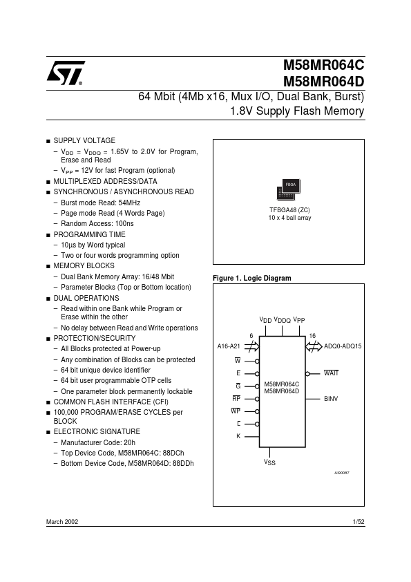
MEMORY BLOCKS – Dual Bank Memory Array: 16/48 Mbit – Parameter Blocks (Top or Bottom location) Figure 1. Logic Diagram
s
DUAL OPERATIONS – Read within one Bank while Program or Erase within the other – No delay between Read and Write operations
VDD VDDQ VPP 6 A16-A21 W E G RP WP L K M58MR064C M58MR064D BINV WAIT 16 ADQ0-ADQ15
s
PROTECTION/SECURITY – All Blocks protected at Power-up – Any combination of Blocks can be protected – 64 bit unique device identifier – 64 bit user programmable OTP cells – One parameter block permanently lockable
s s
COMMON FLASH INTERFACE (CFI) 100,000 PROGRAM/ERASE CYCLES per BLOCK ELECTRONIC SIGNATURE – Manufacturer Code: 20h – Top Device Code, M58MR064C: 88DCh – Bottom Device Code, M58MR064D: 88DDh
s
VSS
AI90087
March 2002
1/52
M58MR064C, M58MR064D
Figure 2. TFBGA Connections (Top view through package)
1
2
3
4
5
6
7
8
9
10
11
12
13
14
A
DU
DU
B
DU
DU
C
WAIT
A21
VSS
K
VDD
W
VPP
A19
A17
NC
D
VDDQ
A16
A20
L
BINV
RP
WP
A18
E
VSS
E
VS...