M58MR032C M58MR032D
32 Mbit (2Mb x16, Mux I/O, Dual Bank, Burst) 1.8V Supply Flash Memory
PRELIMINARY DATA
s
SUPPLY VOL...
M58MR032C M58MR032D
32 Mbit (2Mb x16, Mux I/O, Dual Bank, Burst) 1.8V Supply Flash Memory
PRELIMINARY DATA
s
SUPPLY
VOLTAGE – VDD = VDDQ = 1.7V to 2.0V for Program, Erase and Read
s s
– VPP = 12V for fast Program (optional) MULTIPLEXED ADDRESS/DATA SYNCHRONOUS / ASYNCHRONOUS READ – Burst mode Read: 40MHz – Page mode Read (4 Words Page) – Random Access: 100ns
FBGA
TFBGA48 (ZC) 10 x 4 ball array
s
PROGRAMMING TIME – 10µs by Word typical – Two or four words programming option
s
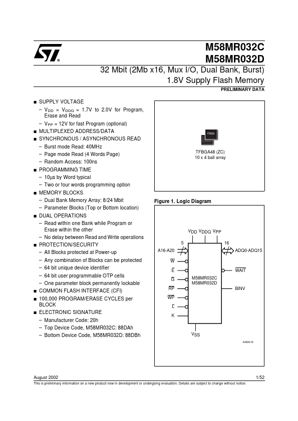
MEMORY BLOCKS – Dual Bank Memory Array: 8/24 Mbit – Parameter Blocks (Top or Bottom location) Figure 1. Logic Diagram
s
DUAL OPERATIONS – Read within one Bank while Program or Erase within the other – No delay between Read and Write operations
VDD VDDQ VPP 5 A16-A20 W E G RP WP L K M58MR032C M58MR032D BINV WAIT 16 ADQ0-ADQ15
s
PROTECTION/SECURITY – All Blocks protected at Power-up – Any combination of Blocks can be protected – 64 bit unique device identifier – 64 bit user programmable OTP cells – One parameter block permanently lockable
s s
COMMON FLASH INTERFACE (CFI) 100,000 PROGRAM/ERASE CYCLES per BLOCK ELECTRONIC SIGNATURE – Manufacturer Code: 20h – Top Device Code, M58MR032C: 88DAh – Bottom Device Code, M58MR032D: 88DBh
s
VSS
AI90019
August 2002
This is preliminary information on a new product now in development or undergoing evaluation. Details are subject to change without notice.
1/52
M58MR032C, M58MR032D
Figure 2. TFBGA Connections (Top view through package)
1
2
3
4
5
6...