M48Z2M1 M48Z2M1Y
16 Mb (2Mb x 8) ZEROPOWER® SRAM
INTEGRATED LOW POWER SRAM, POWER-FAIL CONTROL CIRCUIT and BATTERIES CON...
M48Z2M1 M48Z2M1Y
16 Mb (2Mb x 8) ZEROPOWER® SRAM
INTEGRATED LOW POWER SRAM, POWER-FAIL CONTROL CIRCUIT and BATTERIES CONVENTIONAL SRAM OPERATION; UNLIMITED WRITE CYCLES 10 YEARS of DATA RETENTION in the ABSENCE of POWER AUTOMATIC POWER-FAIL CHIP DESELECT and WRITE PROTECTION WRITE PROTECT
VOLTAGES (VPFD = Power-fail Deselect
Voltage): – M48Z2M1: 4.5V ≤ VPFD ≤ 4.75V – M48Z2M1Y: 4.2V ≤ VPFD ≤ 4.50V BATTERIES ARE INTERNALLY ISOLATED UNTIL POWER IS APPLIED PIN and FUNCTION COMPATIBLE with JEDEC STANDARD 2Mb x 8 SRAMs DESCRIPTION The M48Z2M1/2M1Y ZEROPOWER® RAM is a non-volatile 16,777,216 bit Static RAM organized as 2,097,152 words by 8 bits. The device combines two internal lithium batteries,
CMOS SRAMs and a control circuit in a plastic 36 pin DIP long Module. The ZEROPOWER RAM replaces industry standard SRAMs. It provides the nonvolatility of PROMs without any requirement for special write timing or limitations on the number of writes that can be performed. Table 1. Signal Names
A0-A20 DQ0-DQ7 E G W VCC VSS January 1998
This is preliminary information on a new product now in development or undergoing evaluation. Details are subject to change without notice.
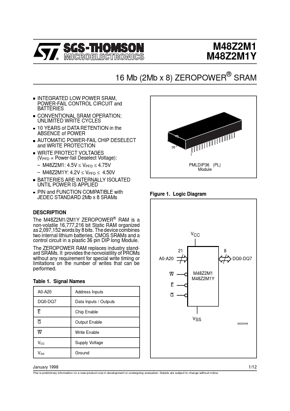
36 1
PMLDIP36 (PL) Module
Figure 1. Logic Diagram
VCC
21 A0-A20 M48Z2M1 M48Z2M1Y
8 DQ0-DQ7
W E G
Address Inputs Data Inputs / Outputs Chip Enable Output Enable Write Enable Supply
Voltage Ground
VSS
AI02048
1/12
M48Z2M1, M48Z2M1Y
Table 2. Absolute Maximum Ratings (1)
Symbol TA TSTG TBIAS TSLD VIO VCC
(2)
Paramet...