16 Mbit 1Mb x16 / Boot Block Flash Memory and 4Mbit 256Kb x16 SRAM / Multiple Memory Product
M36W416TG M36W416BG
16 Mbit (1Mb x16, Boot Block) Flash Memory and 4Mbit (256Kb x16) SRAM, Multiple Memory Product
PRELI...
M36W416TG M36W416BG
16 Mbit (1Mb x16, Boot Block) Flash Memory and 4Mbit (256Kb x16) SRAM, Multiple Memory Product
PRELIMINARY DATA
FEATURES SUMMARY s MULTIPLE MEMORY PRODUCT – 16 Mbit (1Mb x 16) Boot Block Flash Memory – 4 Mbit (256Kb x 16) SRAM s SUPPLY
VOLTAGE – VDDF = VDDS = 2.7V to 3.3V – VDDQF = VDDS = 2.7V to 3.3V – VPPF = 12V for Fast Program (optional)
s s s
SRAM s 4 Mbit (256Kb x 16)
s s s
ACCESS TIME: 70ns LOW VDDS DATA RETENTION: 1.5V POWER DOWN FEATURES USING TWO CHIP ENABLE INPUTS
ACCESS TIME: 70ns, 85ns LOW POWER CONSUMPTION ELECTRONIC SIGNATURE – Manufacturer Code: 20h – Top Device Code, M36W416TG: 88CEh – Bottom Device Code, M36W416BG: 88CFh
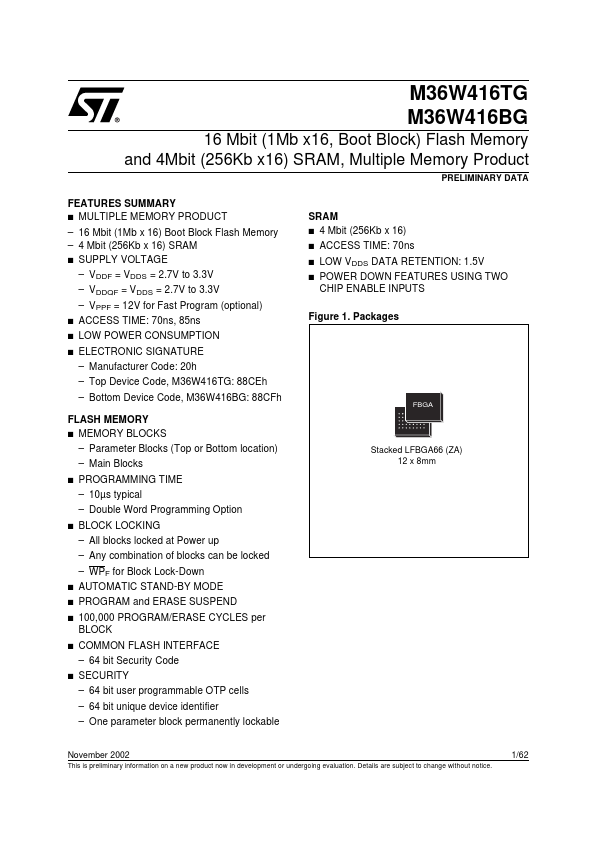
Figure 1. Packages
FBGA
FLASH MEMORY s MEMORY BLOCKS – Parameter Blocks (Top or Bottom location) – Main Blocks
s
Stacked LFBGA66 (ZA) 12 x 8mm
PROGRAMMING TIME – 10µs typical – Double Word Programming Option
s
BLOCK LOCKING – All blocks locked at Power up – Any combination of blocks can be locked – WPF for Block Lock-Down
s s s
AUTOMATIC STAND-BY MODE PROGRAM and ERASE SUSPEND 100,000 PROGRAM/ERASE CYCLES per BLOCK COMMON FLASH INTERFACE – 64 bit Security Code SECURITY – 64 bit user programmable OTP cells – 64 bit unique device identifier – One parameter block permanently lockable
s
s
November 2002
This is preliminary information on a new product now in development or undergoing evaluation. Details are subject to change without notice.
1/62
M36W416TG, M36W416BG
TABLE OF CONTENTS SUMMARY DESCRIPTION . . ....