®
M3493B2
CMOS 12 X 8 CROSSPOINT WITH CONTROL MEMORY
. . . . . . .
LOW ON RESISTANCE (typ. 60 Ω at VDD = 10 V) INTER...
®
M3493B2
CMOS 12 X 8 CROSSPOINT WITH CONTROL MEMORY
. . . . . . .
LOW ON RESISTANCE (typ. 60 Ω at VDD = 10 V) INTERNAL CONTROL LATCHES ANALOGSIGNALSWING CAPABILITYEQUAL TO POWER SUPPLY
VOLTAGE APPLIED LESS THAN 1 % TOTAL DISTORT. AT 0 dBm LESS THAN – 95 dB CROSS-TALK AT 1 KHz 1 VPP VERY LOW POWER CONSUMPTION PIN-TO-PIN COMPATIBLE WITH M093
DIP40
ORDERING NUMBER : M3493B2 (*) (*) It substitutes the obsolete M3493B1.
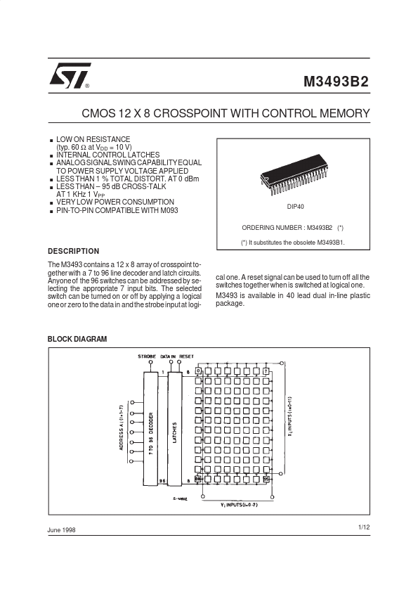
DESCRIPTION The M3493 contains a 12 x 8 array of crosspoint together with a 7 to 96 line decoder and latch circuits. Anyoneof the 96 switches can be addressed by selecting the appropriate 7 input bits. The selected switch can be turned on or off by applying a logical oneor zero to the data in and the strobeinputat logi-
cal one. A reset signal can be used to turn off all the switches together when is switched at logical one. M3493 is available in 40 lead dual in-line plastic package.
BLOCK DIAGRAM
June 1998
1/12
M3493B2
PIN CONNECTION (top view)
INPUT/OUTPUT DESCRIPTION
I/O POWER I I ADDRESS I I AX0-AX3 AY0-AY2 4, 5, 22, 23 2, 24, 25 X Address Lines. These 4 pins are used to select one of the 12 rows of switches. Refer to the truth table for legal address. Y Address Lines. These 3 pins are used to select one of the 8 columns of switches. Refer to the truth table for legal address. VDD VSS 40 20 Positive Power Supply Negative Power Supply Symbol Pin Description
CONTROL I DATA 38 This input determines if the selected switch will be turned on (closed) o...