64M bit Synchronous DRAM
SDRAM (Rev.1.2) Apr. '99
64M bit Synchronous DRAM
MITSUBISHI LSIs
M2V64S20BTP-7,-7L,-8,-8L,-8A,-10,-10L (4-BANK x 419...
Description
SDRAM (Rev.1.2) Apr. '99
64M bit Synchronous DRAM
MITSUBISHI LSIs
M2V64S20BTP-7,-7L,-8,-8L,-8A,-10,-10L (4-BANK x 4194304-WORD x 4-BIT) M2V64S30BTP-7,-7L,-8,-8L,-8A,-10,-10L (4-BANK x 2097152-WORD x 8-BIT) M2V64S40BTP-7,-7L,-8,-8L,-8A,-10,-10L (4-BANK x 1048576-WORD x 16-BIT)
DESCRIPTION
The M2V64S20BTP is organized as 4-bank x 4194304-word x 4-bit, M2V64S30BTP is organized as 4-bank x 2097152-word x 8-bit, and M2V64S40BTP is organized as 4-bank x 1048576-word x 16-bit Synchronous DRAM with LVTTL interface. All inputs and outputs are referenced to the rising edge of CLK. The M2V64S20BTP, M2V64S30BTP, M2V64S40BTP achieve very high speed data rate up to 125MHz, and are suitable for main memory or graphic memory in computer systems.
FEATURES
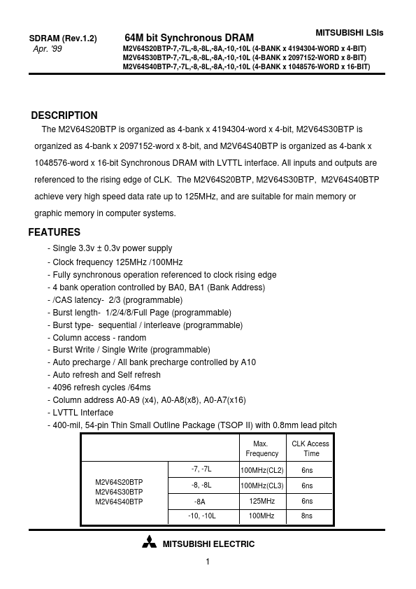
- Single 3.3v ± 0.3v power supply - Clock frequency 125MHz /100MHz - Fully synchronous operation referenced to clock rising edge - 4 bank operation controlled by BA0, BA1 (Bank Address) - /CAS latency- 2/3 (programmable) - Burst length- 1/2/4/8/Full Page (programmable) - Burst type- sequential / interleave (programmable) - Column access - random - Burst Write / Single Write (programmable) - Auto precharge / All bank precharge controlled by A10 - Auto refresh and Self refresh - 4096 refresh cycles /64ms - Column address A0-A9 (x4), A0-A8(x8), A0-A7(x16) - LVTTL Interface - 400-mil, 54-pin Thin Small Outline Package (TSOP II) with 0.8mm lead pitch
Max. Frequency -7, -7L M2V64S20BTP M2V64S30BTP M2V64S40BTP -8, -8L -8A -10, -10L 100MHz(CL2)...
Similar Datasheet