M29W017D
16 Mbit (2Mb x8, Uniform Block) 3V Supply Flash Memory
PRELIMINARY DATA
FEATURES SUMMARY s SUPPLY VOLTAGE – VC...
M29W017D
16 Mbit (2Mb x8, Uniform Block) 3V Supply Flash Memory
PRELIMINARY DATA
FEATURES SUMMARY s SUPPLY
VOLTAGE – VCC = 2.7V to 3.6V for Program, Erase and Read
s s
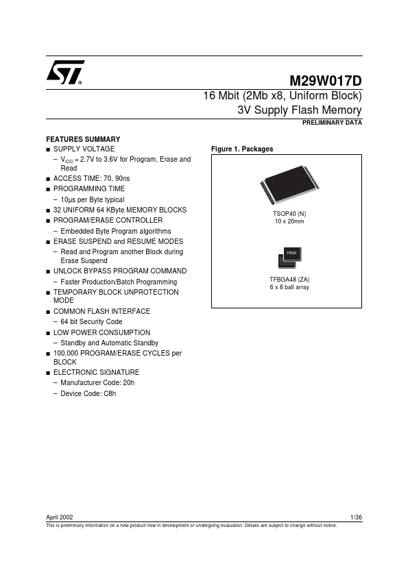
Figure 1. Packages
ACCESS TIME: 70, 90ns PROGRAMMING TIME – 10µs per Byte typical 32 UNIFORM 64 KByte MEMORY BLOCKS PROGRAM/ERASE CONTROLLER – Embedded Byte Program algorithms ERASE SUSPEND and RESUME MODES – Read and Program another Block during Erase Suspend
FBGA
s s
TSOP40 (N) 10 x 20mm
s
s
UNLOCK BYPASS PROGRAM COMMAND – Faster Production/Batch Programming TEMPORARY BLOCK UNPROTECTION MODE COMMON FLASH INTERFACE – 64 bit Security Code LOW POWER CONSUMPTION – Standby and Automatic Standby 100,000 PROGRAM/ERASE CYCLES per BLOCK ELECTRONIC SIGNATURE – Manufacturer Code: 20h – Device Code: C8h
TFBGA48 (ZA) 6 x 8 ball array
s
s
s
s
s
April 2002
This is preliminary information on a new product now in development or undergoing evaluation. Details are subject to change without notice.
1/36
M29W017D
TABLE OF CONTENTS SUMMARY DESCRIPTION . . . . . . . . . . . . . . . . . . . . . . . . . . . . . . . . . . . . . . . . . . . . . . . . . . . . . . . . . . . 5 Figure 2. Logic Diagram . . . . . . . . . . . . . . . . . . . . . . . . . . . . . . . . . . . . . . . . . . . . . . . . . . . . . . . . . . 5 Table 1. Signal Names . . . . . . . . . . . . . . . . . . . . . . . . . . . . . . . . . . . . . . . . . . . . . . . . . . . . . . . . . . . 5 Figure 3. TSOP Connections. . . . . . . . . . . . . . . . . . . . . ...