www.DataSheet4U.com
Integrated Circuit Systems, Inc.
Product Data Sheet
M1025/26
VCSO BASED CLOCK PLL WITH AUTOSWITC...
www.DataSheet4U.com
Integrated Circuit Systems, Inc.
Product Data Sheet
M1025/26
VCSO BASED CLOCK PLL WITH AUTOSWITCH
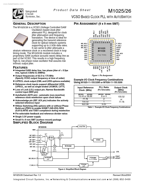
PIN ASSIGNMENT (9 x 9 mm SMT)
MR_SEL3 GND NC DIF_REF0 nDIF_REF0 REF_SEL DIF_REF1 nDIF_REF1 VCC MR_SEL2 MR_SEL0 MR_SEL1 LOL NBW VCC DNC DNC DNC 27 26 25 24 23 22 21 20 19
GENERAL DESCRIPTION
The M1025/26 is a VCSO (
Voltage Controlled SAW Oscillator) based clock jitter attenuator PLL designed for clock jitter attenuation and frequency translation. The device is ideal for generating the transmit reference clock for optical network systems supporting up to 2.5Gb data rates. It can serve to jitter attenuate a stratum reference clock or a recovered clock in loop timing mode. The M1025/26 module includes a proprietary SAW (surface acoustic wave) delay line as part of the VCSO. This results in a high frequency, high-Q, low phase noise oscillator that assures low intrinsic output jitter.
◆ Integrated SAW delay line; low phase jitter of < 0.5ps rms, typical (12kHz to 20MHz) ◆ Output frequencies of 62.5 to 175 MHz (Specify VCSO output frequency at time of order) ◆ LVPECL clock output (CML and LVDS options available) ◆ Reference clock inputs support differential LVDS, LVPECL, as well as single-ended LV
CMOS, LVTTL ◆ Loss of Lock (LOL) output pin; Narrow Bandwidth control input (NBW pin) ◆ AutoSwitch (AUTO pin) - automatic (non-revertive) reference clock reselection upon clock failure ◆ Acknowledge pin (REF_ACK pin) indicates the actively selected reference input ◆ Hit...