Clock Conditioner
LMK03000, LMK03000C, LMK03000D, LMK03001 LMK03001C, LMK03001D, LMK03033, LMK03033C
www.ti.com
SNAS381O – NOVEMBER 2006...
Description
LMK03000, LMK03000C, LMK03000D, LMK03001 LMK03001C, LMK03001D, LMK03033, LMK03033C
www.ti.com
SNAS381O – NOVEMBER 2006 – REVISED MARCH 2013
LMK03000 Family Precision Clock Conditioner with Integrated VCO
Check for Samples: LMK03000, LMK03000C, LMK03000D, LMK03001, LMK03001C, LMK03001D, LMK03033, LMK03033C
1 FEATURES
12
Integrated VCO with Very Low Phase Noise Floor
Integrated Integer-N PLL with Outstanding Normalized Phase Noise Contribution of -224 dBc/Hz
VCO Divider Values of 2 to 8 (All Divides)
Channel Divider Values of 1, 2 to 510 (even divides)
LVDS and LVPECL Clock Outputs
Partially Integrated Loop Filter Dedicated Divider and Delay Blocks on Each
Clock Output Pin Compatible Family of Clocking Devices 3.15 to 3.45 V Operation Package: 48 Pin WQFN (7.0 x 7.0 x 0.8 mm) 200 fs RMS Clock Generator Performance (10
Hz to 20 MHz) with a Clean Input Clock
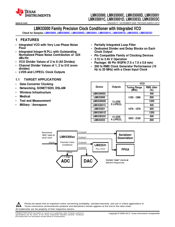
1.1 TARGET APPLICATIONS Data Converter Clocking Networking, SONET/SDH, DSLAM Wireless Infrastructure Medical Test and Measurement Military / Aerospace
Device
LMK03000C LMK03000 LMK03000D LMK03001C LMK03001 LMK03001D LMK03033C LMK03033
Outputs
3 LVDS 5 LVPECL
4 LVDS 4 LVPECL
VCO
Tuning Range RMS Jitter
(MHz)
(fs)
400
1185 - 1296
800
1200
400
1470 - 1570
800
1200
1843 - 2160
500 800
Recovered ³GLUW\´ FORFN RU clean clock
OSCin
CLKout0
LMK0300xx CLKout1
Precision Clock Conditioner
CLKout4 CLKout7
Fout
LMX2531
PLL+VCO
Serializer/ Deserializer
FPGA
> 1 Gsps
ADC
DAC...
Similar Datasheet