Ordering number : EN5787
CMOS IC
LC99063-LF2
CCD Digital Signal Processing IC
Overview
The LC99063-LF2 is a color vid...
Ordering number : EN5787
CMOS IC
LC99063-LF2
CCD Digital Signal Processing IC
Overview
The LC99063-LF2 is a color video signal processor for use with the LC9997M/FL.
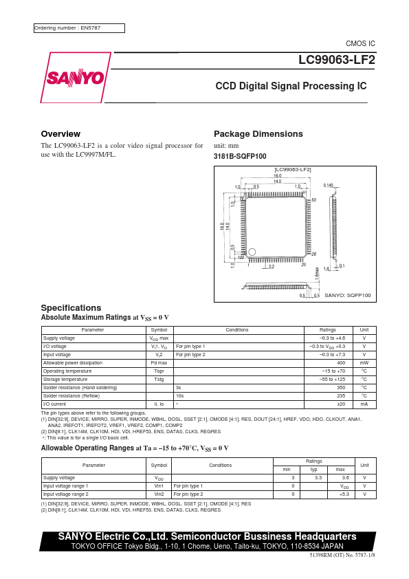
Package Dimensions
unit: mm 3181B-SQFP100
[LC99063-LF2]
SANYO: SQFP100
Specifications
Absolute Maximum Ratings at VSS = 0 V
Parameter Supply
voltage I/O
voltage Input
voltage Allowable power dissipation Operating temperature Storage temperature Solder resistance (Hand soldering) Solder resistance (Reflow) I/O current Ii, Io Symbol VDD max VI1, VO VI2 Pd max Topr Tstg 3s 10s * For pin type 1 For pin type 2 Conditions Ratings –0.3 to +4.6 –0.3 to VDD +0.3 –0.3 to +7.3 400 –15 to +70 –55 to +125 350 235 ±20 Unit V V V mW °C °C °C °C mA
The pin types above refer to the following groups. (1) DIN[32:9], DEVICE, MIRRO, SUPER, INMODE, WBHL, DOSL, SSET [2:1], OMODE [4:1], RES, DOUT [24:1], HREF, VDO, HDO, CLKOUT, ANA1, ANA2, IREFOT1, IREFOT2, VREF1, VREF2, COMP1, COMP2 (2) DIN[8:1], CLK14M, CLK10M, HDI, VDI, HREF53, ENS, DATAS, CLKS, REGRES *: This value is for a single I/O basic cell.
Allowable Operating Ranges at Ta = –15 to +70°C, VSS = 0 V
Parameter Supply
voltage Input
voltage range 1 Input
voltage range 2 Symbol VDD Vin1 Vin2 For pin type 1 For pin type 2 Conditions Ratings min 3 0 0 typ 3.3 max 3.6 VDD +5.3 Unit V V V
(1) DIN[32:9], DEVICE, MIRRO, SUPER, INMODE, WBHL, DOSL, SSET [2:1], OMODE [4:1], RES (2) DIN[8:1], CLK14M, CLK10M, HDI, VDI, HREF53, ENS, DATAS, CLKS, REGRES
SANYO Electric Co.,Ltd. Semicon...