Ordering number : EN5545
MOS LSI
LC89977M
CCD Delay Line for PAL
Preliminary Overview
The LC89977M is CCD delay line f...
Ordering number : EN5545
MOS LSI
LC89977M
CCD Delay Line for PAL
Preliminary Overview
The LC89977M is CCD delay line for PAL television system that includes a chrominance signal crosstalk exclusion filter and a luminance signal 1-H delay line on chip.
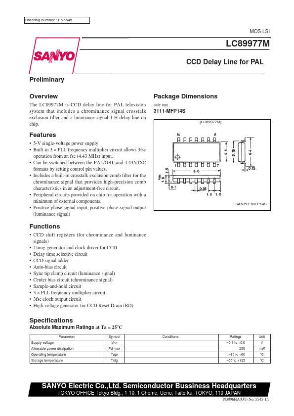
Package Dimensions
unit: mm
3111-MFP14S
[LC89977M]
Features
5-V single-
voltage power supply Built-in 3 × PLL frequency multiplier circuit allows 3fsc operation from an fsc (4.43 MHz) input. Can be switched between the PAL/GBI, and 4.43NTSC formats by setting control pin values. Includes a built-in crosstalk exclusion comb filter for the chrominance signal that provides high-precision comb characteristics in an adjustment-free circuit. Peripheral circuits provided on chip for operation with a minimum of external components. Positive-phase signal input, positive-phase signal output (luminance signal)
SANYO: MFP14S
Functions
CCD shift registers (for chrominance and luminance signals) Timig generator and clock driver for CCD Delay time selective circuit CCD signal adder Auto-bias circuit Sync tip clamp circuit (luminance signal) Center bias circuit (chrominance signal) Sample-and-hold circuit 3 × PLL frequency multiplier circuit 3fsc clock output circuit High
voltage generator for CCD Reset Drain (RD)
Specifications
Absolute Maximum Ratings at Ta = 25°C
Parameter Supply
voltage Allowable power dissipation Operating temperature Storage temperature Symbol VDD Pd max Topr Tstg Conditions Rating...