LESHAN RADIO COMPANY, LTD.
2-Input AND Gate
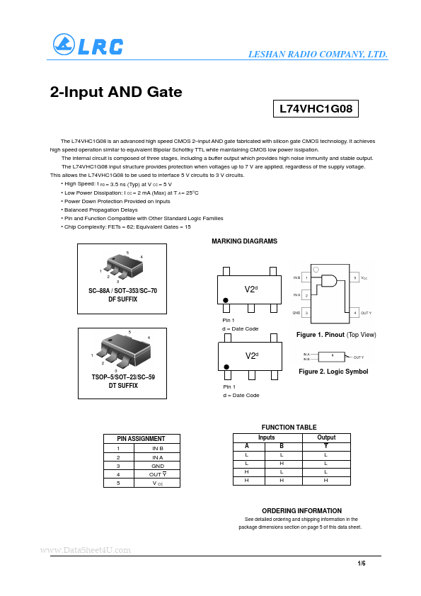
L74VHC1G08
The L74VHC1G08 is an advanced high speed CMOS 2–input AND gate f...
LESHAN RADIO COMPANY, LTD.
2-Input AND Gate
L74VHC1G08
The L74VHC1G08 is an advanced high speed
CMOS 2–input AND gate fabricated with silicon gate
CMOS technology. It achieves high speed operation similar to equivalent Bipolar Schottky TTL while maintaining
CMOS low power issipation. The internal circuit is composed of three stages, including a buffer output which provides high noise immunity and stable output. The L74VHC1G08 input structure provides protection when
voltages up to 7 V are applied, regardless of the supply
voltage. This allows the L74VHC1G08 to be used to interface 5 V circuits to 3 V circuits. High Speed: t PD = 3.5 ns (Typ) at V CC = 5 V Low Power Dissipation: I CC = 2 mA (Max) at T A = 25°C Power Down Protection Provided on Inputs Balanced Propagation Delays Pin and Function Compatible with Other Standard Logic Families Chip Complexity: FETs = 62; Equivalent Gates = 15
MARKING DIAGRAMS
5 4 1 2 3
SC–88A / SOT–353/SC–70 DF SUFFIX
V2d
5 4
Pin 1 d = Date Code
Figure 1. Pinout (Top View)
1 2 3
V2d
Figure 2. Logic Symbol
Pin 1 d = Date Code
TSOP–5/SOT–23/SC–59 DT SUFFIX
FUNCTION TABLE
PIN ASSIGNMENT 1 2 3 4 5 IN B IN A GND OUT Y V CC A L L H H Inputs B L H L H Output Y L L L H
ORDERING INFORMATION
See detailed ordering and shipping information in the package dimensions section on page 5 of this data sheet.
www.DataSheet4U.com
1/6
LESHAN RADIO COMPANY, LTD.
L74VHC1G08
MAXIMUM RATINGS
Value Unit – 0.5 to + 7.0 V – 0.5 to 7.0 V V CC=0 – 0.5...