KSC5321
KSC5321
High Voltage and High Reliability
• High speed Switching • Wide Safe Operating Area
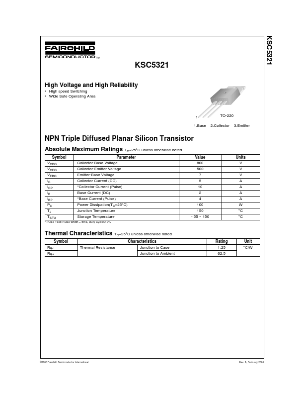
1
TO-220 2.Collec...
KSC5321
KSC5321
High
Voltage and High Reliability
High speed Switching Wide Safe Operating Area
1
TO-220 2.Collector 3.Emitter
1.Base
NPN Triple Diffused Planar Silicon Transistor
Absolute Maximum Ratings TC=25°C unless otherwise noted
Symbol VCBO VCEO VEBO IC ICP IB IBP PC TJ TSTG Parameter Collector-Base
Voltage Collector-Emitter
Voltage Emitter-Base
Voltage Collector Current (DC) *Collector Current (Pulse) Base Current (DC) *Base Current (Pulse) Power Dissipation(TC=25°C) Junction Temperature Storage Temperature Value 800 500 7 5 10 2 4 100 150 - 55 ~ 150 Units V V V A A A A W °C °C
* Pulse Test: Pulse Width = 5ms, Duty Cycle≤10%
Thermal Characteristics TC=25°C unless otherwise noted
Symbol Rθjc Rθja Thermal Resistance Characteristics Junction to Case Junction to Ambient Rating 1.25 62.5 Unit °C/W
©2000 Fairchild Semiconductor International
Rev. A, February 2000
KSC5321
Electrical Characteristics TC=25°C unless otherwise noted
Symbol BVCBO BVCEO BVEBO ICBO IEBO hFE1 hFE2 VCE(sat) VBE(sat) fT Cob Cib tON tSTG tF tON tSTG tF Parameter Collector-Base Breakdown
Voltage Collector-Emitter Breakdown
Voltage Emitter-Base Breakdown
Voltage Collector Cut-off Current Emitter Cut-off Current DC Current Gain Collector-Emitter Saturation
Voltage Base-Emitter Saturation
Voltage Current Gain bandwidth Product Output Capacitance Input Capacitance Turn ON Time Storage Time Fall Time Turn ON Time Storage Time Fall Time Test Condition IC = 1mA, IE = 0 IC = 5mA, IB = 0 IC =1mA, ...