www.DataSheet4U.com
TECHNICAL DATA
KK4503B
Hex Buffer
High-Voltage Silicon-Gate CMOS
The KK4503B is a hex noninvertin...
www.DataSheet4U.com
TECHNICAL DATA
KK4503B
Hex Buffer
High-
Voltage Silicon-Gate
CMOS
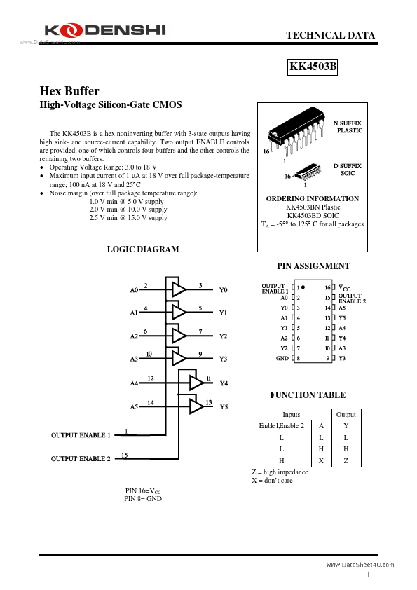
The KK4503B is a hex noninverting buffer with 3-state outputs having high sink- and source-current capability. Two output ENABLE controls are provided, one of which controls four buffers and the other controls the remaining two buffers. Operating
Voltage Range: 3.0 to 18 V Maximum input current of 1 µA at 18 V over full package-temperature range; 100 nA at 18 V and 25°C Noise margin (over full package temperature range): 1.0 V min @ 5.0 V supply 2.0 V min @ 10.0 V supply 2.5 V min @ 15.0 V supply
ORDERING INFORMATION KK4503BN Plastic KK4503BD SOIC TA = -55° to 125° C for all packages
LOGIC DIAGRAM PIN ASSIGNMENT
FUNCTION TABLE
Inputs Enable 1,Enable 2 L L H Z = high impedance X = don’t care PIN 16=VCC PIN 8= GND A L H X Output Y L H Z
1
www.DataSheet4U.com
KK4503B
MAXIMUM RATINGS*
Symbol VCC VIN VOUT IIN PD PD Tstg TL
*
Parameter DC Supply
Voltage (Referenced to GND) DC Input
Voltage (Referenced to GND) DC Output
Voltage (Referenced to GND) DC Input Current, per Pin Power Dissipation in Still Air, Plastic DIP+ SOIC Package+ Power Dissipation per Output Transistor Storage Temperature Lead Temperature, 1 mm from Case for 10 Seconds (Plastic DIP or SOIC Package)
Value -0.5 to +20 -0.5 to VCC +0.5 -0.5 to VCC +0.5 ±10 750 500 100 -65 to +150 260
Unit V V V mA mW mW °C °C
Maximum Ratings are those values beyond which damage to the device may occur. Functional operation should b...