www.DataSheet4U.com
TECHNICAL DATA
KK4502B
Strobed Hex Inverter/Buffer
High-Voltage Silicon-Gate CMOS
The KK4502B con...
www.DataSheet4U.com
TECHNICAL DATA
KK4502B
Strobed Hex Inverter/Buffer
High-
Voltage Silicon-Gate
CMOS
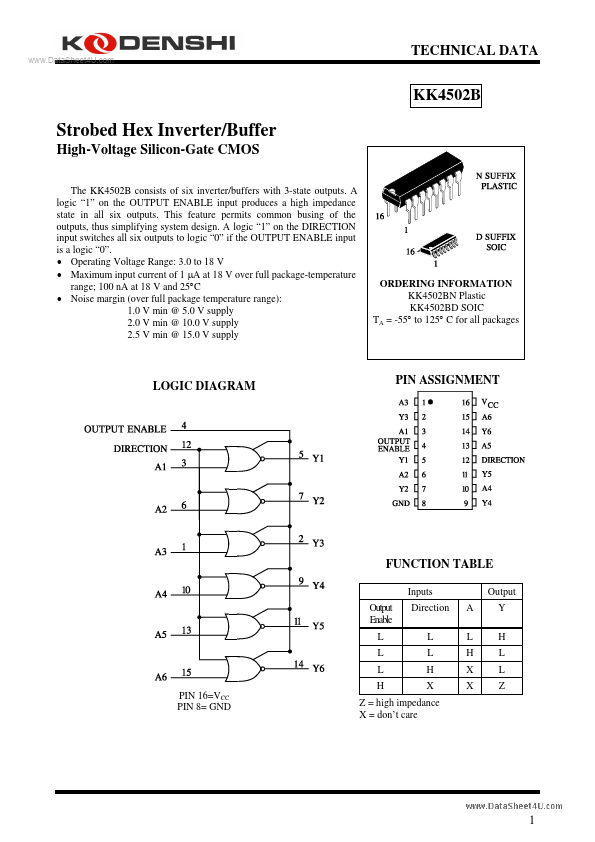
The KK4502B consists of six inverter/buffers with 3-state outputs. A logic “1” on the OUTPUT ENABLE input produces a high impedance state in all six outputs. This feature permits common busing of the outputs, thus simplifying system design. A logic “1” on the DIRECTION input switches all six outputs to logic “0” if the OUTPUT ENABLE input is a logic “0”. Operating
Voltage Range: 3.0 to 18 V Maximum input current of 1 µA at 18 V over full package-temperature range; 100 nA at 18 V and 25°C Noise margin (over full package temperature range): 1.0 V min @ 5.0 V supply 2.0 V min @ 10.0 V supply 2.5 V min @ 15.0 V supply
ORDERING INFORMATION KK4502BN Plastic KK4502BD SOIC TA = -55° to 125° C for all packages
LOGIC DIAGRAM
PIN ASSIGNMENT
FUNCTION TABLE
Inputs Output Enable L L L H PIN 16=VCC PIN 8= GND Direction L L H X A L H X X Output Y H L L Z
Z = high impedance X = don’t care
1
www.DataSheet4U.com
KK4502B
MAXIMUM RATINGS*
Symbol VCC VIN VOUT IIN PD PD Tstg TL
*
Parameter DC Supply
Voltage (Referenced to GND) DC Input
Voltage (Referenced to GND) DC Output
Voltage (Referenced to GND) DC Input Current, per Pin Power Dissipation in Still Air, Plastic DIP+ SOIC Package+ Power Dissipation per Output Transistor Storage Temperature Lead Temperature, 1 mm from Case for 10 Seconds (Plastic DIP or SOIC Package)
Value -0.5 to +20 -0.5 to VCC +0.5 -0.5 to VCC +0.5 ±10 750 ...