www.DataSheet4U.com
TECHNICAL DATA
KK4042B
Quad Clocked «D» Latch
High-Voltage Silicon-Gate CMOS
KK4042B types contai...
www.DataSheet4U.com
TECHNICAL DATA
KK4042B
Quad Clocked «D» Latch
High-
Voltage Silicon-Gate
CMOS
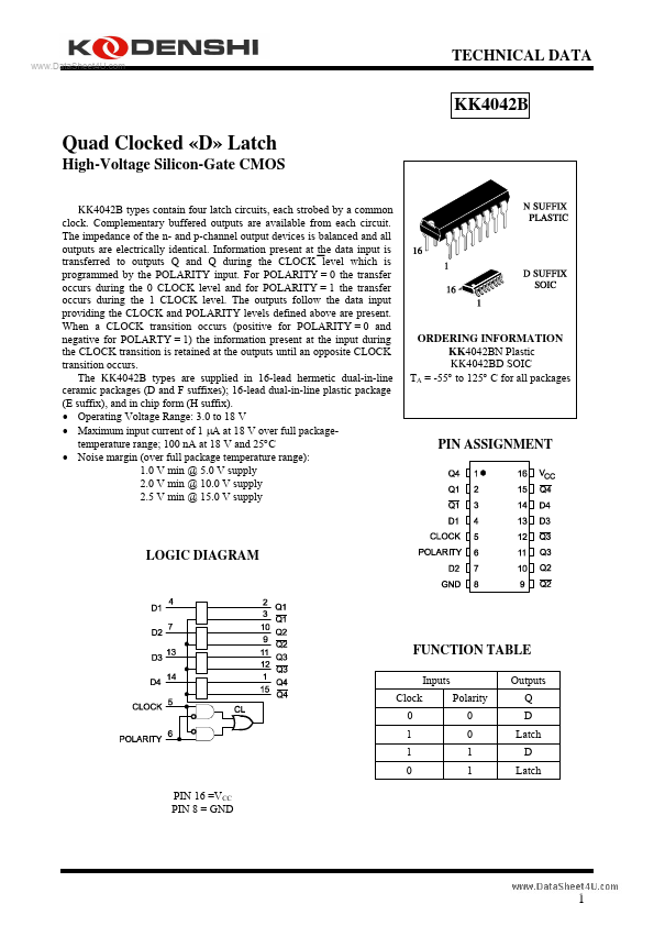
KK4042B types contain four latch circuits, each strobed by a common clock. Complementary buffered outputs are available from each circuit. The impedance of the n- and p-channel output devices is balanced and all outputs are electrically identical. Information present at the data input is transferred to outputs Q and Q during the CLOCK level which is programmed by the POLARITY input. For POLARITY = 0 the transfer occurs during the 0 CLOCK level and for POLARITY = 1 the transfer occurs during the 1 CLOCK level. The outputs follow the data input providing the CLOCK and POLARITY levels defined above are present. When a CLOCK transition occurs (positive for POLARITY = 0 and negative for POLARTY = 1) the information present at the input during the CLOCK transition is retained at the outputs until an opposite CLOCK transition occurs. The KK4042B types are supplied in 16-lead hermetic dual-in-line ceramic packages (D and F suffixes); 16-lead dual-in-line plastic package (E suffix), and in chip form (H suffix). Operating
Voltage Range: 3.0 to 18 V Maximum input current of 1 µA at 18 V over full packagetemperature range; 100 nA at 18 V and 25°C Noise margin (over full package temperature range): 1.0 V min @ 5.0 V supply 2.0 V min @ 10.0 V supply 2.5 V min @ 15.0 V supply
ORDERING INFORMATION KK4042BN Plastic KK4042BD SOIC TA = -55° to 125° C for all packages
PIN ASSIGNMENT
LOGIC...