www.DataSheet4U.com
TECHNICAL DATA
KK4040B
12-Stage Binary Ripple Counter
High-Voltage Silicon-Gate CMOS
The KK4040B ...
www.DataSheet4U.com
TECHNICAL DATA
KK4040B
12-Stage Binary Ripple Counter
High-
Voltage Silicon-Gate
CMOS
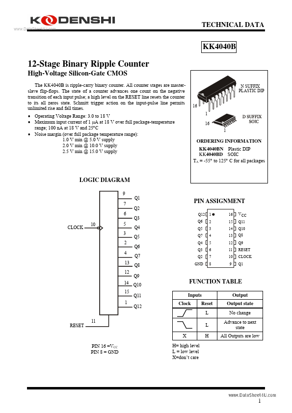
The KK4040B is ripple-carry binary counter. All counter stages are masterslave flip-flops. The state of a counter advances one count on the negative transition of each input pulse; a high level on the RESET line resets the counter to its all zeros state. Schmitt trigger action on the input-pulse line permits unlimited rise and fall times. Operating
Voltage Range: 3.0 to 18 V Maximum input current of 1 µA at 18 V over full package-temperature range; 100 nA at 18 V and 25°C Noise margin (over full package temperature range): 1.0 V min @ 5.0 V supply 2.0 V min @ 10.0 V supply 2.5 V min @ 15.0 V supply
N SUFFIX PLASTIC DIP 16 1 16 1
ORDERING INFORMATION
KK4040BN Plastic DIP KK4040BD SOIC TA = -55° to 125° C for all packages
LOGIC DIAGRAM
9 7 6 CLOCK 10 5 3 2 4 13 12 14 15 1 Q1 Q2 Q3 Q4 Q5 Q6 Q7 Q8 Q9 Q10 Q11 Q12
Q12 Q6 Q5 Q7 Q4 Q3 Q2 GND
PIN ASSIGNMENT
1 2 3 4 5 6 7 8 16 15 14 13 12 11 10 9
V CC Q11 Q10 Q8 Q9 RESET CLOCK Q1
FUNCTION TABLE
Inputs
Clock Reset
L
Output
Output state
No change
Advance to next state
All Outputs are low
RESET
11
L
X H
PIN 16 =VCC PIN 8 = GND
H= high level L = low level X=don’t care
1
www.DataSheet4U.com
KK4040B
MAXIMUM RATINGS*
Symbol VCC VIN VOUT IIN PD Ptot Tstg TL
*
Parameter DC Supply
Voltage (Referenced to GND) DC Input
Voltage (Referenced to GND) DC Output
Voltage (Referenced to GND) DC Input Current, per Pin Power Dissi...