(K7J161882B / K7J163682B) 512Kx36 & 1Mx18 DDR II SIO b2 SRAM
K7J163682B K7J161882B www.DataSheet4U.com
Document Title
512Kx36 & 1Mx18 DDR II SIO b2 SRAM
512Kx36-bit, 1Mx18-bit DDR...
Description
K7J163682B K7J161882B www.DataSheet4U.com
Document Title
512Kx36 & 1Mx18 DDR II SIO b2 SRAM
512Kx36-bit, 1Mx18-bit DDR II SIO b2 SRAM
Revision History
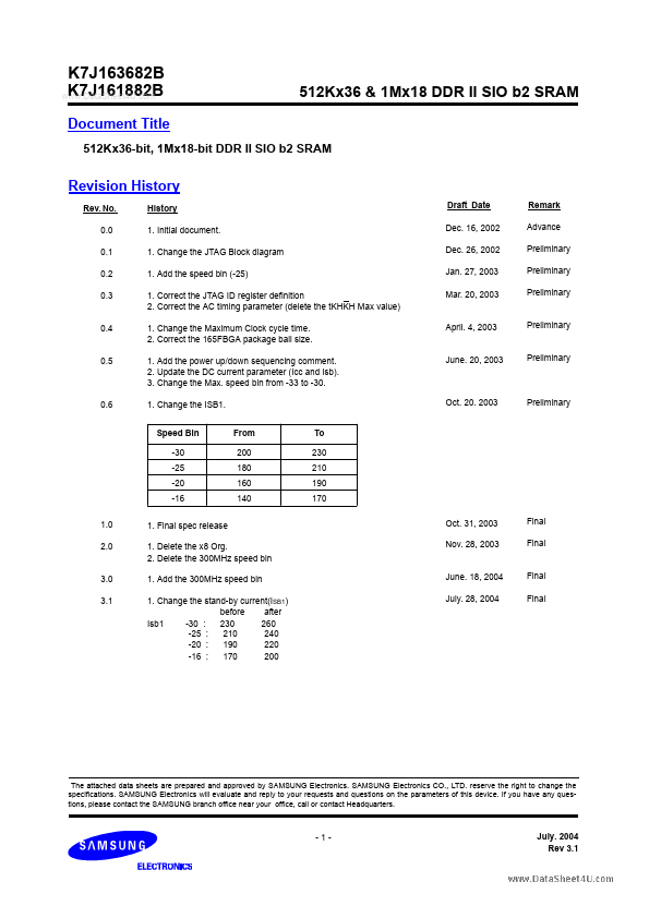
Rev. No. 0.0 0.1 0.2 0.3 History 1. Initial document. 1. Change the JTAG Block diagram 1. Add the speed bin (-25) 1. Correct the JTAG ID register definition 2. Correct the AC timing parameter (delete the tKHKH Max value) 1. Change the Maximum Clock cycle time. 2. Correct the 165FBGA package ball size. 1. Add the power up/down sequencing comment. 2. Update the DC current parameter (Icc and Isb). 3. Change the Max. speed bin from -33 to -30. 1. Change the ISB1. Speed Bin -30 -25 -20 -16 1.0 2.0 1. Final spec release 1. Delete the x8 Org. 2. Delete the 300MHz speed bin 1. Add the 300MHz speed bin 1. Change the stand-by current(ISB1) before after Isb1 -30 : 230 260 -25 : 210 240 -20 : 190 220 -16 : 170 200 From 200 180 160 140 To 230 210 190 170 Oct. 31, 2003 Nov. 28, 2003 Final Final Draft Date Dec. 16, 2002 Dec. 26, 2002 Jan. 27, 2003 Mar. 20, 2003 Remark Advance Preliminary Preliminary Preliminary
0.4
April. 4, 2003
Preliminary
0.5
June. 20, 2003
Preliminary
0.6
Oct. 20. 2003
Preliminary
3.0 3.1
June. 18, 2004 July. 28, 2004
Final Final
The attached data sheets are prepared and approved by SAMSUNG Electronics. SAMSUNG Electronics CO., LTD. reserve the right to change the specifications. SAMSUNG Electronics will evaluate and reply to your requests and questions on the parameters of this device. If you have any que...
Similar Datasheet