2SK1404
Silicon N-Channel MOS FET
Application
High speed power switching
Features
Low on-resistance High speed switching Low drive current No secondary breakdown Suitable for switching regulator and DC-DC converter
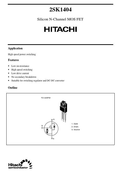
Outline
TO-220FM
D G
1
2 3
1. Gate 2. Drain 3. Source
S
2SK1404
Absolute Maximum Ratings (Ta = 25°C)
Item Drain to source vol...