2SK1310A
TOSHIBA FIELD EFFECT TRANSISTOR SILICON N CHANNEL MOS TYPE
2SK1310A
RF POWER MOS FET for VHF TV BROADCAST TRANSMITTER
z Output Power
: Po ≥ 190 W (Min.)
z Drain Efficiency
: ηD = 65% (Typ.)
z Frequency
: f = 230 MHz
z Push−Pull Structure Package
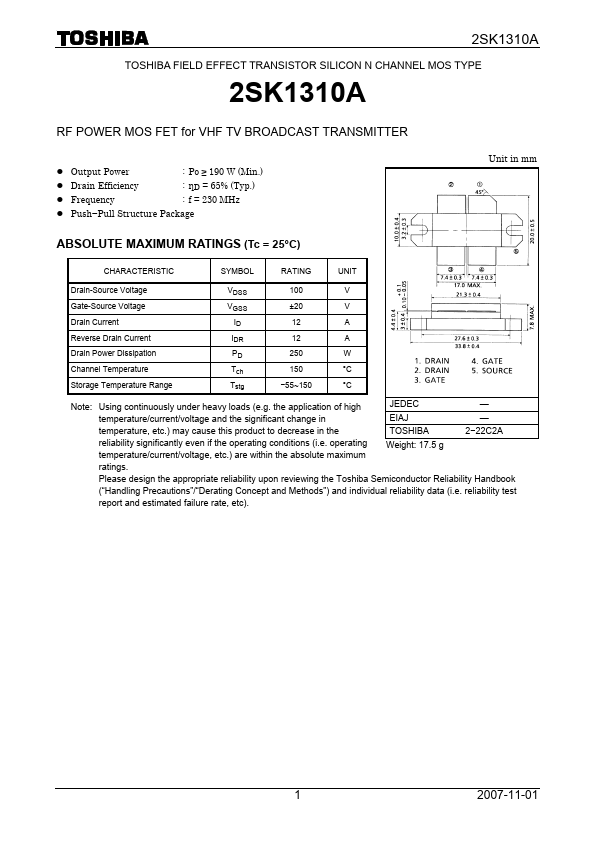
Unit in mm
ABSOLUTE MAXIMUM RATINGS (Tc = 25°C)
CHARACTERISTIC
SYMBOL
RATING
UNIT
Drain-So...