www.DataSheet4U.com
K1300 Series
5V Crystal Clock Oscillators
! ! ! ! ! ! TTL/CMOS Compatible Tri-State Feature for Aut...
www.DataSheet4U.com
K1300 Series
5V Crystal Clock Oscillators
! ! ! ! ! ! TTL/
CMOS Compatible Tri-State Feature for Auto Test Systems Fast Rise and Fall Times 70 to 120 MHz Frequency Range Tight Symmetry (45/55%) Available
±100ppm Stability Standard ±50ppm Stability Available - K1350
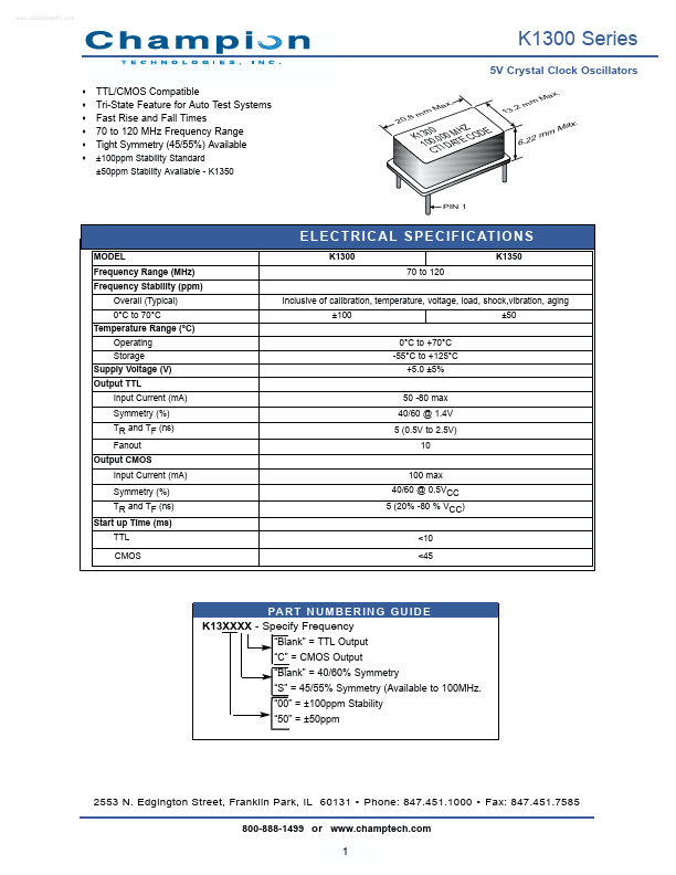
ax. mM m 8 20, ax. mM m 2 13,
00 00 MHZCODE K130 0 1 0.TI DATE C
m 2m 6,2
x. Ma
PIN 1
E L E C T R I C A L S P E C I F I C AT I O N S
MODEL Frequency Range (MHz) Frequency Stability (ppm) Overall (Typical) 0°C to 70°C Temperature Range (°C) Operating Storage Supply
Voltage (V) Output TTL Input Current (mA) Symmetry (%) TR and TF (ns) Fanout Output
CMOS Input Current (mA) Symmetry (%) TR and TF (ns) Start up Time (ms) TTL
CMOS <10 <45 100 max 40/60 @ 0.5VCC 5 (20% -80 % VCC) 50 -80 max 40/60 @ 1.4V 5 (0.5V to 2.5V) 10 0°C to +70°C -55°C to +125°C +5.0 ±5% Inclusive of calibration, temperature,
voltage, load, shock,vibration, aging ±100 ±50 K1300 70 to 120 K1350
PA R T N U M B E R I N G G U I D E K13XXXX - Specify Frequency
“Blank” = TTL Output “C” =
CMOS Output “Blank” = 40/60% Symmetry “S” = 45/55% Symmetry (Available to 100MHz. “00” = ±100ppm Stability “50” = ±50ppm
2553 N. Edgington Street, Franklin Park, IL 60131 " Phone: 847.451.1000 " Fax: 847.451.7585 800-888-1499 or www.champtech.com
1
K1300 Series
5V Crystal Clock Oscillators
PIN 1 2 3 4 FUNCTION Tri-State* Ground Output + VCC
* Input tied internally to +5V. External input if any, should not be less than +3V and not greater than...