2SK1153, 2SK1154
Silicon N-Channel MOS FET
Application
High speed power switching
Features
• Low on-resistance • High sp...
2SK1153, 2SK1154
Silicon N-Channel MOS FET
Application
High speed power switching
Features
Low on-resistance High speed switching Low drive current No secondary breakdown Suitable for switching regulator and DC-DC converter
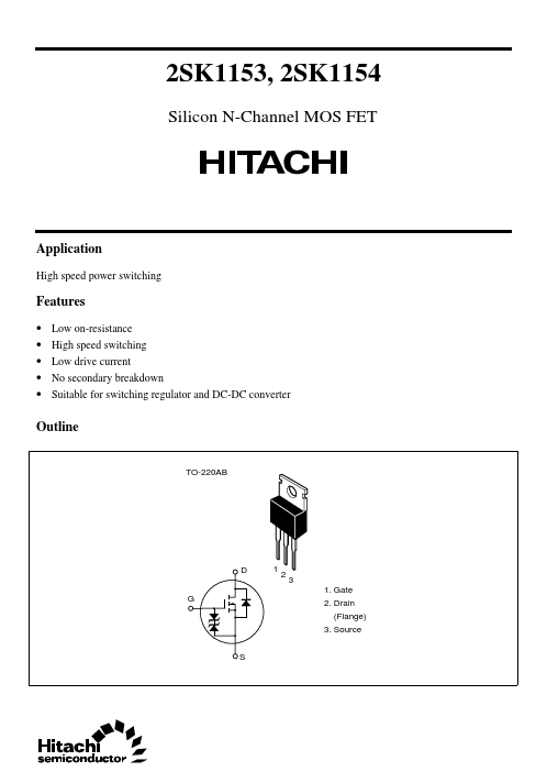
Outline
TO-220AB
D 123 1. Gate
G 2. Drain (Flange)
3. Source S
2SK1153, 2SK1154
Absolute Maximum Ratings (Ta = 25°C)
Item
Drain to source
voltage
2SK1153
2SK1154
Gate to source
voltage
Drain current
Drain peak current
Body to drain diode reverse drain current
Channel dissipation
Channel temperature
Storage temperature
Notes: 1. PW ≤ 10 µs, duty cycle ≤ 1% 2. Value at TC = 25°C
Symbol VDSS
VGSS ID I *1
D(pulse)
I DR Pch*2 Tch Tstg
Ratings 450 500 ±30 3 12 3 30 150 –55 to +150
Unit V
V A A A W °C °C
2
2SK1153, 2SK1154
Electrical Characteristics (Ta = 25°C)
Item
Symbol Min
Drain to source breakdown
voltage
2SK1153 V(BR)DSS 2SK1154
450 500
Gate to source breakdown
voltage
V(BR)GSS ±30
Gate to source leak current
I GSS
Zero gate
voltage 2SK1153 IDSS
drain current
2SK1154
— —
Gate to source cutoff
voltage VGS(off) Static Drain to source 2SK1153 RDS(on) on stateresistance 2SK1154
2.0 — —
Forward transfer admittance |yfs|
1.5
Input capacitance
Ciss —
Output capacitance
Coss —
Reverse transfer capacitance Crss —
Turn-on delay time Rise time Turn-off delay time Fall time Body to drain diode forward
voltage
t d(on) tr t d(off) tf VDF
— — — — —
Body to drain diode reverse recovery time
t rr
—
Note: 1. Pulse te...