TECHNICAL DATA
IW4081B
Quad 2-Input AND Gate
High-Voltage Silicon-Gate CMOS
The IW4081B AND gates provide the system d...
TECHNICAL DATA
IW4081B
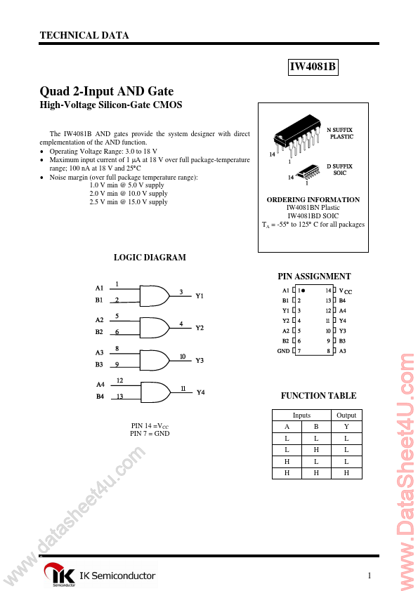
Quad 2-Input AND Gate
High-
Voltage Silicon-Gate
CMOS
The IW4081B AND gates provide the system designer with direct emplementation of the AND function. Operating
Voltage Range: 3.0 to 18 V Maximum input current of 1 µA at 18 V over full package-temperature range; 100 nA at 18 V and 25°C Noise margin (over full package temperature range): 1.0 V min @ 5.0 V supply 2.0 V min @ 10.0 V supply 2.5 V min @ 15.0 V supply
ORDERING INFORMATION IW4081BN Plastic IW4081BD SOIC TA = -55° to 125° C for all packages
LOGIC DIAGRAM PIN ASSIGNMENT
FUNCTION TABLE
Inputs PIN 14 =VCC PIN 7 = GND A L L H H B L H L H Output Y L L L H
w
w
w
.d
e e h s a t a
. u t4
m o c
1
www.DataSheet4U.com
IW4081B
MAXIMUM RATINGS*
Symbol VCC VIN VOUT IIN PD PD Tstg TL
*
Parameter DC Supply
Voltage (Referenced to GND) DC Input
Voltage (Referenced to GND) DC Output
Voltage (Referenced to GND) DC Input Current, per Pin Power Dissipation in Still Air, Plastic DIP+ SOIC Package+ Power Dissipation per Output Transistor Storage Temperature Lead Temperature, 1 mm from Case for 10 Seconds (Plastic DIP or SOIC Package)
Value -0.5 to +20 -0.5 to VCC +0.5 -0.5 to VCC +0.5 ±10 750 500 100 -65 to +150 260
Unit V V V mA mW mW °C °C
Maximum Ratings are those values beyond which damage to the device may occur. Functional operation should be restricted to the Recommended Operating Conditions. +Derating - Plastic DIP: - 10 mW/°C from 65° to 125°C SOIC Package: : - 7 mW/°C from 65° to 12...