DatasheetsPDF.com
IRL520NS
Part Number
IRL520NS
Manufacturer
International Rectifier
Description
Power
MOSFET
Published
Feb 22, 2007
Datasheet
IRL520NS
PDF File
Features
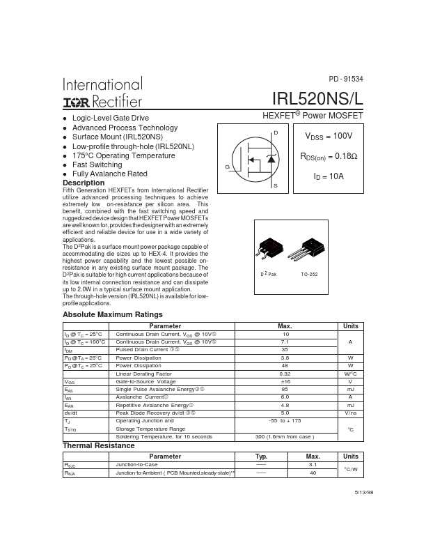
www..com PD - 91534 IRL520NS/L Logic-Level Gate Drive l Advanced Process Technology l Surface Mount (IRL520NS) l Low-profile through-hole (IRL520NL) l 175°C Operating Temperature l Fast
Switching
l Fully Avalanche Rated Description l HE...
Similar Datasheet
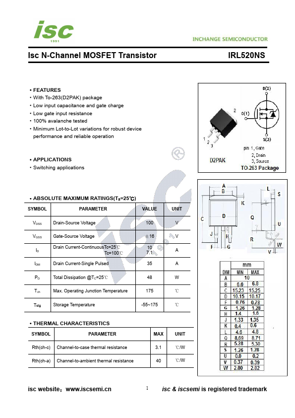
IRL520NS
N-Channel MOSFET
(INCHANGE)
Since 2006. D4U Semicon,
Electronic Components Datasheet Search Site. (
Privacy Policy & Contact
)