IRL520NL Datasheet
Isc N-Channel MOSFET Transistor
·FEATURES ·With To-262 package ·Low input capacitance and gate charge ·Low gate input resistance ·100% avalanche tested ·Minimum Lot-to-Lot variations for robust device
performance and reliable operation
·APPLICATIONS ·Switching applications
·ABSOLUTE MAXIMUM RATINGS(Ta=25℃)
SYMBOL
PARAMETER
VALUE
UNIT
VDSS
Drain-Source Voltage
100
V
VGSS
Gate-Source Voltage
±16
V
ID
Drain Current-ContinuousTc=25℃ Tc=100℃
10 7.1
A
IDM
Drain Current-Single Pulsed
35
A
PD
Total Dissipation @TC=25℃
48
W
Tch
Max. Operating Junction Temperature
175
℃
Tstg
Storage Temperature
-55~175
℃
·THERMAL CHARACTERISTICS
SYMBOL
PARAMETER
MAX
UNIT
Rth(ch-c) Channel-to-case thermal resistance
3.1
℃/W
IRL520NL
isc website:www.iscsemi.cn
1 isc & iscsemi is registered trademark
Isc N-Channel MOSFET Transistor
ELECTRICAL CHARACTERISTICS
TC=25℃ unless otherwise specified
SYMBOL
PARAMETER
CONDITIONS
BVDSS
Drain-Source Breakdown Voltage VGS=0V;.
Part Number |
IRL520NL |
Manufacturers |
International Rectifier |
Logo |
|
Description |
Power MOSFET |
Datasheet |
IRL520NL Datasheet (PDF) |
www.DataSheet4U.com
PD - 91534
IRL520NS/L
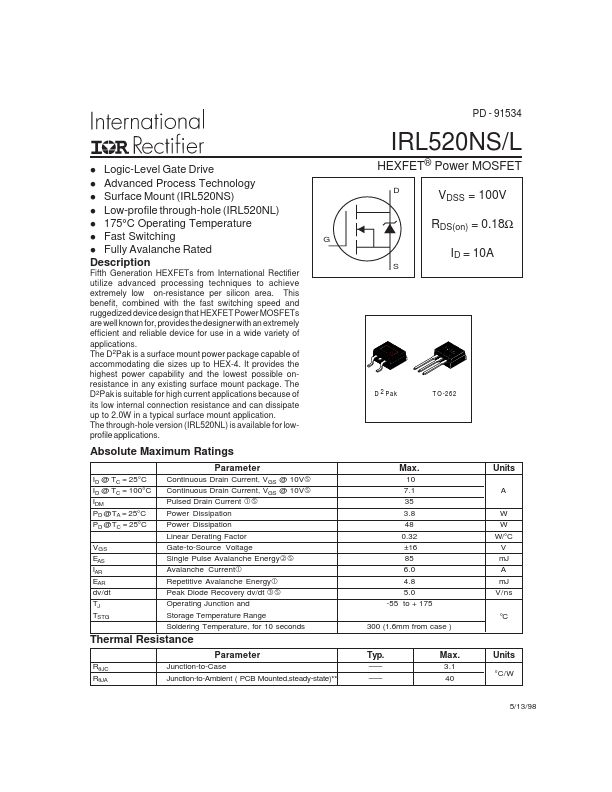
Logic-Level Gate Drive l Advanced Process Technology l Surface Mount (IRL520NS) l Low-profile through-hole (IRL520NL) l 175°C Operating Temperature l Fast Switching l Fully Avalanche Rated Description
l
HEXFET® Power MOSFET
D
VDSS = 100V RDS(on) = 0.18Ω
G
ID = 10A
S
Fifth Generation HEXFETs from International Rectifier utilize advanced processing techniques to achieve extremely low on-resistance per silicon area. This benefit, combined with the fast switching speed and ruggedized device design that HEXFET Power MOSFETs are well known for, provides the designer with an extremely efficient and reliable device for use in a wide variety of applica.
N-Channel MOSFET
Isc N-Channel MOSFET Transistor
·FEATURES ·With To-262 package ·Low input capacitance and gate charge ·Low gate input resistance ·100% avalanche tested ·Minimum Lot-to-Lot variations for robust device
performance and reliable operation
·APPLICATIONS ·Switching applications
·ABSOLUTE MAXIMUM RATINGS(Ta=25℃)
SYMBOL
PARAMETER
VALUE
UNIT
VDSS
Drain-Source Voltage
100
V
VGSS
Gate-Source Voltage
±16
V
ID
Drain Current-ContinuousTc=25℃ Tc=100℃
10 7.1
A
IDM
Drain Current-Single Pulsed
35
A
PD
Total Dissipation @TC=25℃
48
W
Tch
Max. Operating Junction Temperature
175
℃
Tstg
Storage Temperature
-55~175
℃
·THERMAL CHARACTERISTICS
SYMBOL
PARAMETER
MAX
UNIT
Rth(ch-c) Channel-to-case thermal resistance
3.1
℃/W
IRL520NL
isc website:www.iscsemi.cn
1 isc & iscsemi is registered trademark
Isc N-Channel MOSFET Transistor
ELECTRICAL CHARACTERISTICS
TC=25℃ unless otherwise specified
SYMBOL
PARAMETER
CONDITIONS
BVDSS
Drain-Source Breakdown Voltage VGS=0V; ID= 0.25mA
VGS(th)
Gate Threshold Voltage
VDS=VGS; ID=0.25mA
RDS(on) Drain-Source On-Resistance
VGS= 10V; ID=6A
IGSS IDSS VSDF
Gate-Source Leakage Current
VGS= ±16V;VDS= 0V
Drain-Source Leakage Current
VDS=100V; VGS= 0V;Tj=25℃ VDS=80V; VGS= 0V;Tj=125℃
Diode forward voltage
ISD=6.0A, VGS = 0 V
IRL520NL
MIN TYP MAX UNIT
100
V
1.0
2.0
V
180 mΩ
±0.1 μA
25 250
μA
1.3
V
NOTICE: ISC reserves the rights to make changes of the content herein the datasheet at any time without no.
2020-10-31 : IRFU4105 IRFSL7787 IRFSL7762 IRFU5410 IRFU9024N IRFZ45 IRFZ48 IRKD56-14 IRL520NL IRL530NL