PD - 91494A
IRL520N
HEXFET®
l l l l l l
Power MOSFET VDSS = 100V
Logic-Level Gate Drive Advanced Process Technology D...
PD - 91494A
IRL520N
HEXFET®
l l l l l l
Power
MOSFET VDSS = 100V
Logic-Level Gate Drive Advanced Process Technology Dynamic dv/dt Rating 175°C Operating Temperature Fast Switching Fully Avalanche Rated
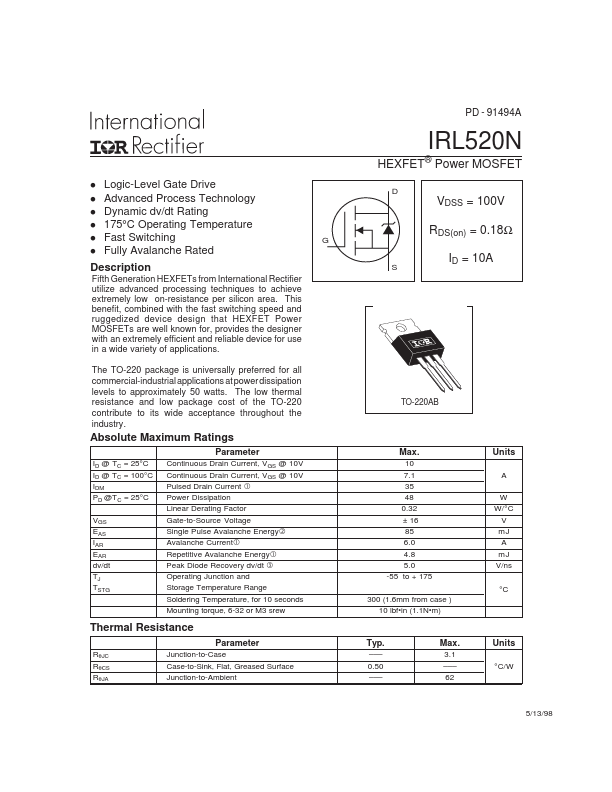
D
G S
RDS(on) = 0.18Ω ID = 10A
Description
Fifth Generation HEXFETs from International Rectifier utilize advanced processing techniques to achieve extremely low on-resistance per silicon area. This benefit, combined with the fast switching speed and ruggedized device design that HEXFET Power
MOSFETs are well known for, provides the designer with an extremely efficient and reliable device for use in a wide variety of applications. The TO-220 package is universally preferred for all commercial-industrial applications at power dissipation levels to approximately 50 watts. The low thermal resistance and low package cost of the TO-220 contribute to its wide acceptance throughout the industry.
TO-220AB
Absolute Maximum Ratings
Parameter
ID @ TC = 25°C ID @ TC = 100°C IDM PD @TC = 25°C VGS EAS IAR EAR dv/dt TJ TSTG Continuous Drain Current, VGS @ 10V Continuous Drain Current, VGS @ 10V Pulsed Drain Current Power Dissipation Linear Derating Factor Gate-to-Source
Voltage Single Pulse Avalanche Energy Avalanche Current Repetitive Avalanche Energy Peak Diode Recovery dv/dt Operating Junction and Storage Temperature Range Soldering Temperature, for 10 seconds Mounting torque, 6-32 or M3 srew
Max.
10 7.1 35 48 0.32 ± 16 85 6.0 4.8 5.0 -55 to + 175 300 (1.6mm from case ) 10 ...