|
Part Number
|
IRL520L |
|
Manufacturer
|
Vishay |
|
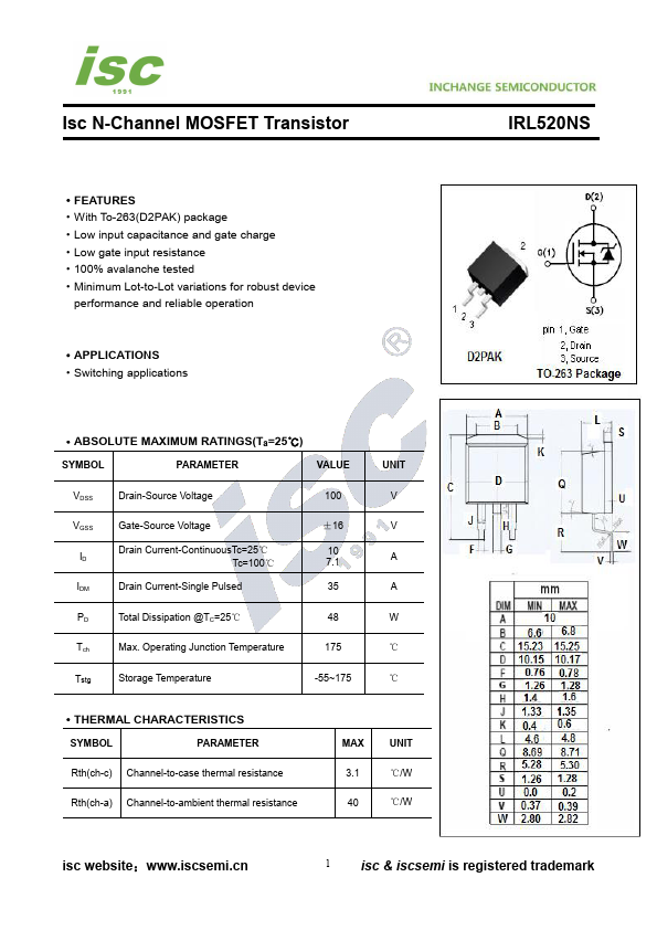
Description
|
Power MOSFET |
|
Published
|
Nov 21, 2015 |
|
Datasheet
|
 IRL520L PDF File IRL520L PDF File
|
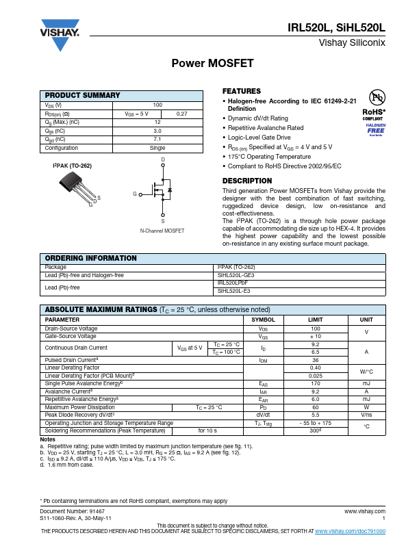
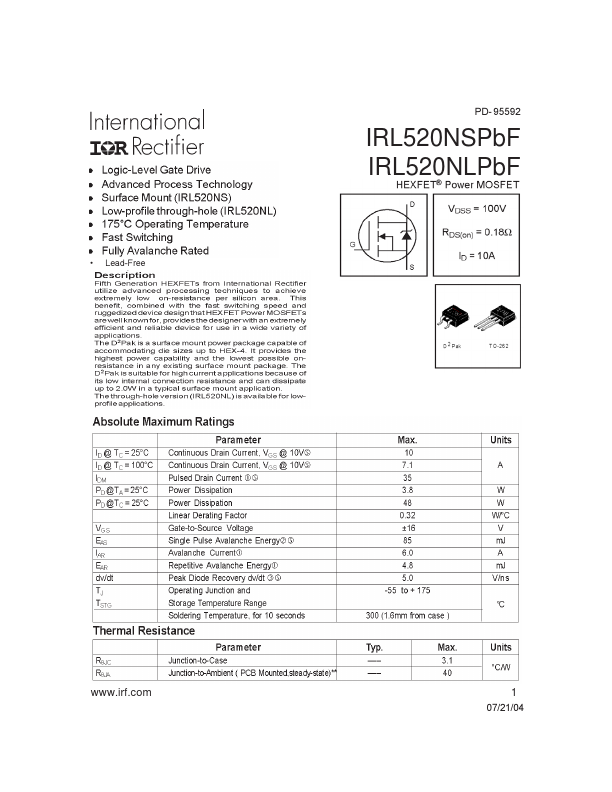
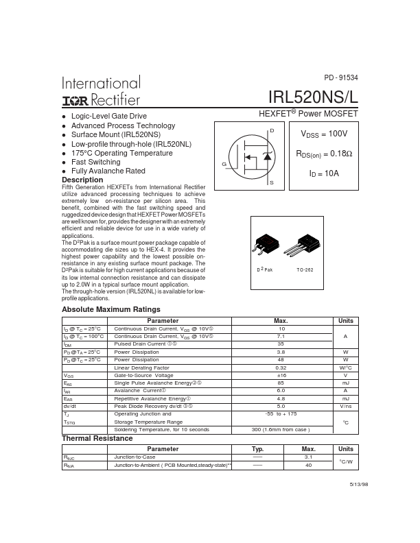
Features
• Halogen-free According to IEC 61249-2-21
Definition
• Dynamic dV/dt Rating
• Repetitive Avalanche Rated
• Logic-Level Gate Drive
• RDS (on) Specified at VGS = 4 V and 5 V
• 175°C Operating Temperature
• Compliant to RoHS Directive 2002/95/EC
DESCRI...
Similar Datasheet
INDEX :57ABCDEFGHIJKLMNOPQRSTUVWXYZ