|
Part Number
|
IRL520A |
|
Manufacturer
|
Fairchild |
|
Description
|
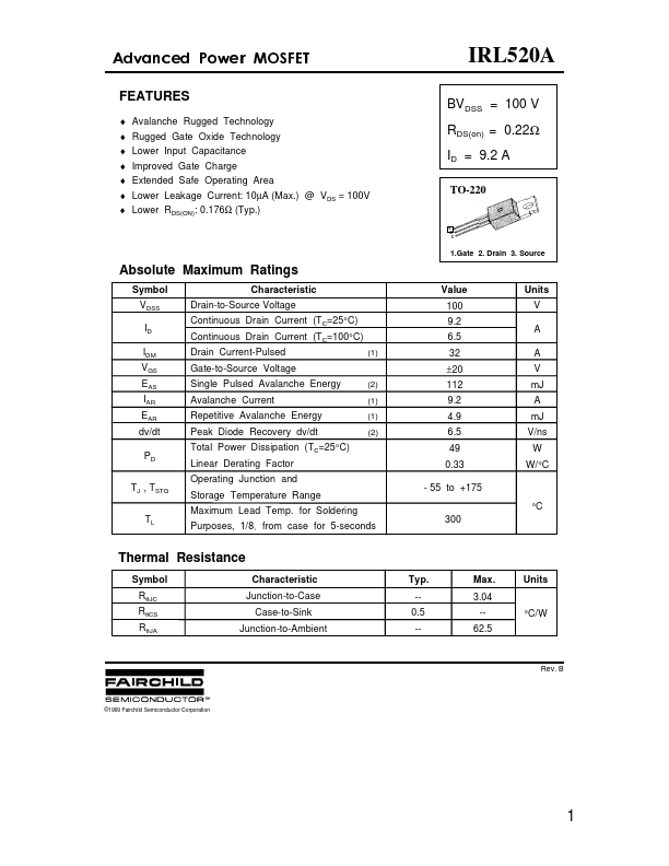
Advenced Power MOSFET |
|
Features
|
♦ Avalanche Rugged Technology ♦ Rugged Gate Oxide Technology ♦ Lower Input Capacitance ♦ Improved Gate Charge ♦ Extended...
|
|
Published
|
Jul 6, 2005 |
|
Datasheet
|
 IRL520A PDF File IRL520A PDF File
|
Features
♦ Avalanche Rugged Technology ♦ Rugged Gate Oxide Technology ♦ Lower Input Capacitance ♦ Improved Gate Charge ♦ Extended Safe Operating Area ♦ Lower Leakage Current: 10µA (Max.) @ VDS = 100V ♦ Lower RDS(ON): 0.176Ω (Typ.)
1 2 3
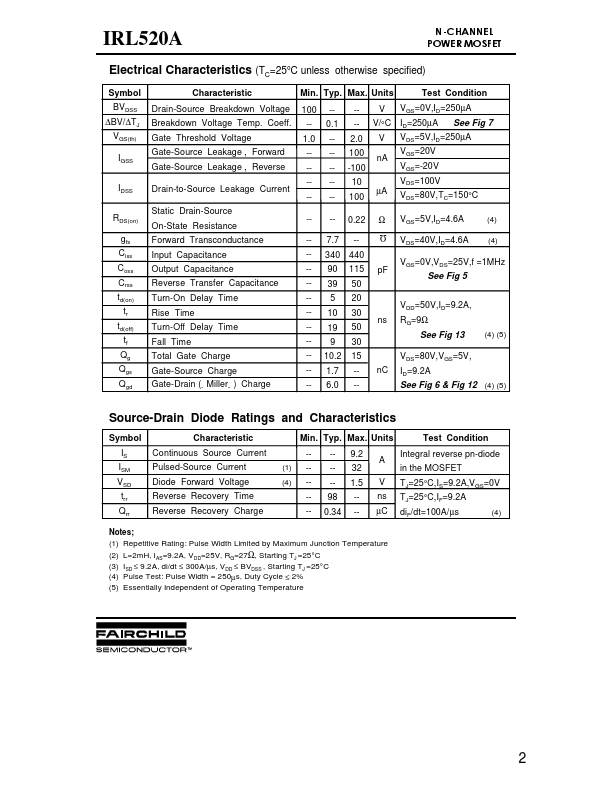
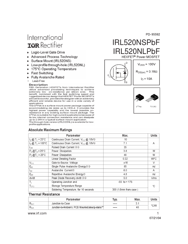
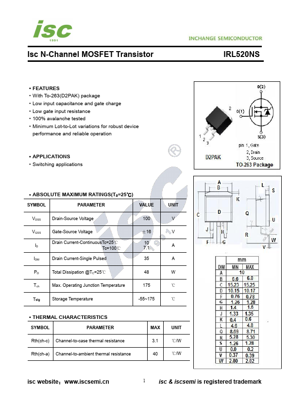
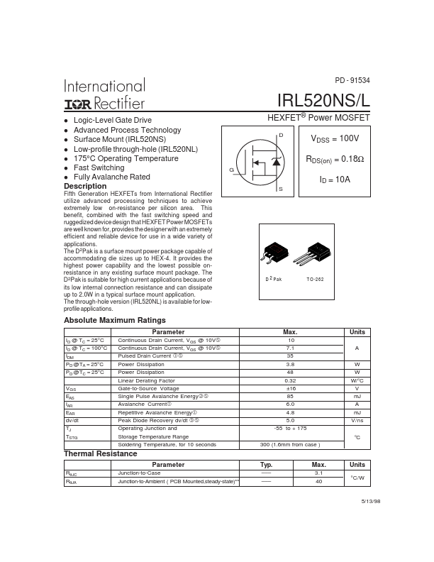
IRL520A
BVDSS = 100 V...
Similar Datasheet
INDEX :57ABCDEFGHIJKLMNOPQRSTUVWXYZ