DatasheetsPDF.com
IRL510A
Advanced Power MOSFET
Description
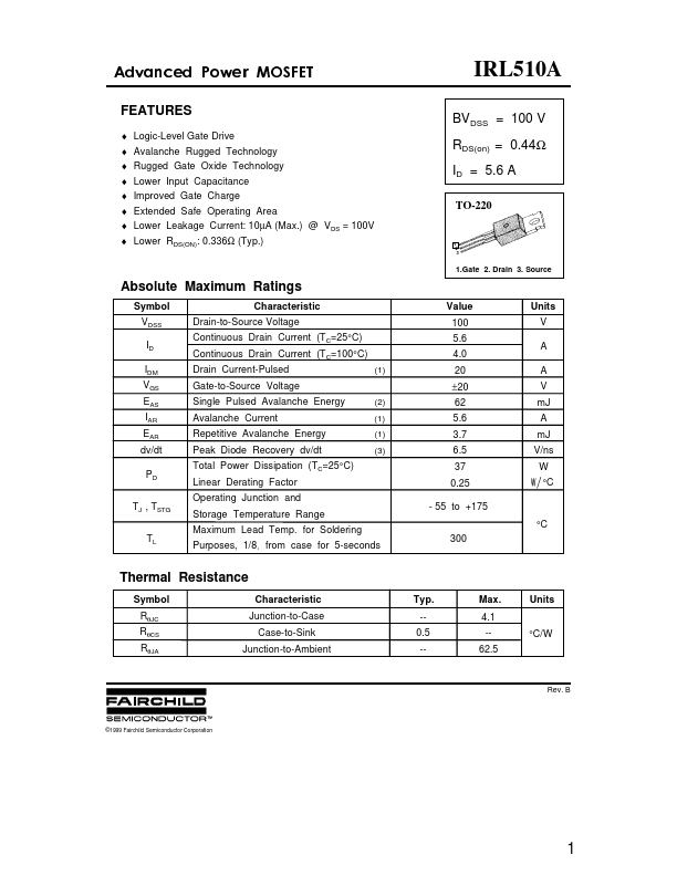
$GYDQFHG 3RZHU 026)(7 FEATURES ♦ Logic-Level Gate Drive ♦ Avalanche Rugged Technology ♦ Rugged Gate Oxide Technology ♦ Lower Input Capacitance ♦ Improved Gate Charge ♦ Extended Safe Operating Area ♦ Lower Leakage Current: 10µA (Max.) @ VDS = 100V ♦ Lower RDS(ON): 0.336Ω (Typ.) IRL510A BVDSS = 100 V RDS(on) = 0.44Ω ID = 5.6 A TO-220 1 2 3 1.Gate 2. Drain 3...
Fairchild
Download IRL510A Datasheet
Similar Datasheet
IRL510S
Power MOSFET
- Vishay
IRL510S
HEXFET POWER MOSFET
- IRF
IRL510
Power MOSFET
- Fairchild Semiconductor
IRL510
Power MOSFET
- Vishay Siliconix
@ 2014 :: Datasheetspdf.com :: Semiconductors datasheet search & download site. (
Privacy Policy & Contact
)