Advanced Power MOSFET
FEATURES
Avalanche Rugged Technology Rugged Gate Oxide Technology Lower Input Capacitance Improved...
Advanced Power
MOSFET
FEATURES
Avalanche Rugged Technology Rugged Gate Oxide Technology Lower Input Capacitance Improved Gate Charge Extended Safe Operating Area 175ΟC Operating Temperature Lower Leakage Current : 10 µ A (Max.) @ VDS = 100V Lower RDS(ON) : 0.289 Ω (Typ.)
Absolute Maximum Ratings
Symbol VDSS
ID
IDM VGS EAS IAR EAR dv/dt
PD
TJ , TSTG
TL
Characteristic
Drain-to-Source
Voltage
Continuous Drain Current (TC=25 ΟC)
Continuous Drain Current (TC=100 ΟC)
Drain Current-Pulsed
O1
Gate-to-Source
Voltage
Single Pulsed Avalanche Energy Avalanche Current Repetitive Avalanche Energy Peak Diode Recovery dv/dt
O2 O1 O1 O3
Total Power Dissipation (TC=25 ΟC) Linear Derating Factor
Operating Junction and
Storage Temperature Range
Maximum Lead Temp. for Soldering
Purposes, 1/8”from case for 5-seconds
IRFS510A
BVDSS = 100 V RDS(on) = 0.4 Ω ID = 4.5 A
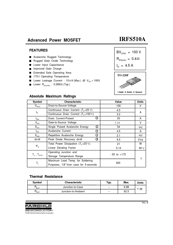
TO-220F
1 2 3
1.Gate 2. Drain 3. Source
Value 100 4.5 3.2 20
+_ 20 54 4.5 2.1 6.5 21 0.14
- 55 to +175
300
Units V
A
A V mJ A mJ V/ns W W/ ΟC
ΟC
Thermal Resistance
Symbol
Rθ JC RθJA
Characteristic Junction-to-Case Junction-to-Ambient
©1999 Fairchild Semiconductor Corporation
Typ. ---
Max. 6.98 62.5
Units ΟC /W
Rev. B
IRFS510A
N-CHANNEL POWER
MOSFET
Electrical Characteristics (TC=25ΟCunless otherwise specified)
Symbol BVDSS
∆BV/ ∆TJ VGS(th)
IGSS
IDSS
RDS(on)
gfs Ciss Coss Crss td(on)
tr td(off)
tf Qg Qgs Qgd
Characteristic
Min. Typ. Max. Units
Test Condition
Drain-Source Breakdown
Voltage Breakdown Vo...