IRFS250B
November 2001
IRFS250B
200V N-Channel MOSFET
General Description
These N-Channel enhancement mode power field...
IRFS250B
November 2001
IRFS250B
200V N-Channel
MOSFET
General Description
These N-Channel enhancement mode power field effect transistors are produced using Fairchild’s proprietary, planar, DMOS technology. This advanced technology has been especially tailored to minimize on-state resistance, provide superior switching performance, and withstand high energy pulse in the avalanche and commutation mode. These devices are well suited for high efficiency switching DC/DC converters, switch mode power supplies, DC-AC converters for uninterrupted power supply and motor control.
Features
21.3A, 200V, RDS(on) = 0.085Ω @VGS = 10 V Low gate charge ( typical 95 nC) Low Crss ( typical 75 pF) Fast switching 100% avalanche tested Improved dv/dt capability
D
!
●
◀
▲
● ●
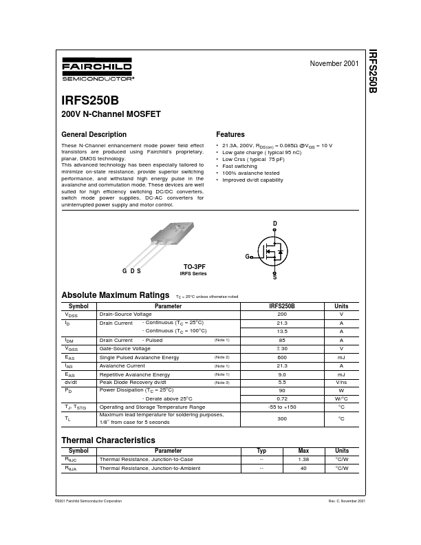
G! G D S
TO-3PF
IRFS Series
!
S
Absolute Maximum Ratings
Symbol VDSS ID IDM VGSS EAS IAR EAR dv/dt PD TJ, TSTG TL
TC = 25°C unless otherwise noted
Parameter Drain-Source
Voltage - Continuous (TC = 25°C) Drain Current - Continuous (TC = 100°C) Drain Current - Pulsed
(Note 1)
IRFS250B 200 21.3 13.5 85 ± 30
(Note 2) (Note 1) (Note 1) (Note 3)
Units V A A A V mJ A mJ V/ns W W/°C °C °C
Gate-Source
Voltage Single Pulsed Avalanche Energy Avalanche Current Repetitive Avalanche Energy Peak Diode Recovery dv/dt Power Dissipation (TC = 25°C)
600 21.3 9.0 5.5 90 0.72 -55 to +150 300
- Derate above 25°C Operating and Storage Temperature Range Maximum lead temperature for soldering purposes, 1/8" from case for ...