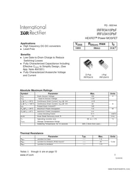
PD - 95514A
IRFR3410PbF IRFU3410PbF
HEXFET® Power MOSFET
Applications High frequency DC-DC converters l Lead-Free
l
VD...
PD - 95514A
IRFR3410PbF IRFU3410PbF
HEXFET® Power
MOSFET
Applications High frequency DC-DC converters l Lead-Free
l
VDSS
100V
RDS(on) max
39mΩ
ID
31A
Benefits Low Gate-to-Drain Charge to Reduce Switching Losses l Fully Characterized Capacitance Including Effective COSS to Simplify Design, (See App. Note AN1001) l Fully Characterized Avalanche
Voltage and Current
l
D-Pak IRFR3410
I-Pak IRFU3410
Absolute Maximum Ratings
Symbol
VDS VGS ID @ TC = 25°C ID @ TC = 100°C IDM PD @TC = 25°C PD @TA = 25°C dv/dt TJ TSTG
Parameter
Drain-Source
Voltage Gate-to-Source
Voltage Continuous Drain Current, VGS @ 10V Continuous Drain Current, VGS @ 10V Pulsed Drain Current Maximum Power Dissipation Maximum Power Dissipation Linear Derating Factor Peak Diode Recovery dv/dt Operating Junction and Storage Temperature Range Soldering Temperature, for 10 seconds
Max.
100 ± 20 31 22 125 110 3.0 0.71 15 -55 to + 175 300 (1.6mm from case )
Units
V
A W mW°C V/ns °C
Thermal Resistance
Parameter
RθJC RθJA RθJA Junction-to-Case Junction-to-Ambient (PCB mount)* Junction-to-Ambient
Typ.
––– ––– –––
Max.
1.4 40 110
Units
°C/W
Notes through are on page 10
www.irf.com
1
12/03/04
IRFR/U3410PbF
Static @ TJ = 25°C (unless otherwise specified)
Parameter Drain-to-Source Breakdown
Voltage ∆V(BR)DSS/∆TJ Breakdown
Voltage Temp. Coefficient RDS(on) Static Drain-to-Source On-Resistance VGS(th) Gate Threshold
Voltage V(BR)DSS IDSS IGSS Drain-to-Source Leakage Current Gate-to-Source Forward Leaka...