VDS VGS max
RDS(on) max
(@VGS = -10V)
Qg (typical)
ID
(@TC = 25°C)
-30 ±20
37
13
d-8.5
V V
mΩ nC A
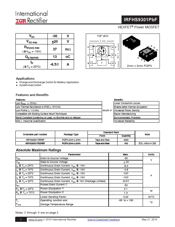
TOP VIEW
IRFHS930...
VDS VGS max
RDS(on) max
(@VGS = -10V)
Qg (typical)
ID
(@TC = 25°C)
-30 ±20
37
13
d-8.5
V V
mΩ nC A
TOP VIEW
IRFHS9301PbF
HEXFET® Power
MOSFET
D1 D2 G3
6D D 5D S 4S
D D
DG
D D S
S
2mm x 2mm PQFN
Applications
l Charge and Discharge Switch for Battery Application l System/load switch
Features and Benefits
Features Low RDSon (≤ 37mΩ) Low Thermal Resistance to PCB (≤ 13°C/W) Low Profile (≤ 1.0 mm) Compatible with Existing Surface Mount Techniques RoHS Compliant Containing no Lead, no Bromide and no Halogen MSL1, Industrial Qualification
results in
Benefits Lower Conduction Losses Enable better thermal dissipation Increased Power Density Easier Manufacturing Environmentally Friendlier Increased Reliability
Orderable part number
IRFHS9301TRPBF IRFHS9301TR2PBF
Package Type
PQFN 2mm x 2mm PQFN 2mm x 2mm
Standard Pack Form Tape and Reel Tape and Reel
Quantity 4000 400
Absolute Maximum Ratings
VDS VGS ID @ TA = 25°C ID @ TA = 70°C ID @ TC = 25°C ID @ TC = 70°C ID @ TC = 25°C IDM PD @TA = 25°C PD @ TA = 70°C
TJ TSTG
Parameter Drain-to-Source
Voltage
Gate-to-Source
Voltage Continuous Drain Current, VGS @ -10V Continuous Drain Current, VGS @ -10V Continuous Drain Current, VGS @ -10V Continuous Drain Current, VGS @ -10V
cContinuous Drain Current, VGS @ 10V (Package Limited)
Pulsed Drain Current
fPower Dissipation fPower Dissipation
Linear Derating Factor Operating Junction and
Storage Temperature Range
Max. -30 ± 20 -6.0 -4.8
-13d -10d d-8.5
-52 2.1 1.3
0.02 -55 to + 15...