PD- 93898A
SMPS MOSFET
Applications l High frequency DC-DC converters
IRF7451
HEXFET® Power MOSFET
VDSS
150V
RDS(on)...
PD- 93898A
SMPS
MOSFET
Applications l High frequency DC-DC converters
IRF7451
HEXFET® Power
MOSFET
VDSS
150V
RDS(on) max
0.09Ω
ID
3.6A
Benefits Low Gate to Drain Charge to Reduce Switching Losses l Fully Characterized Capacitance Including Effective COSS to Simplify Design, (See App. Note AN1001) l Fully Characterized Avalanche
Voltage and Current
l
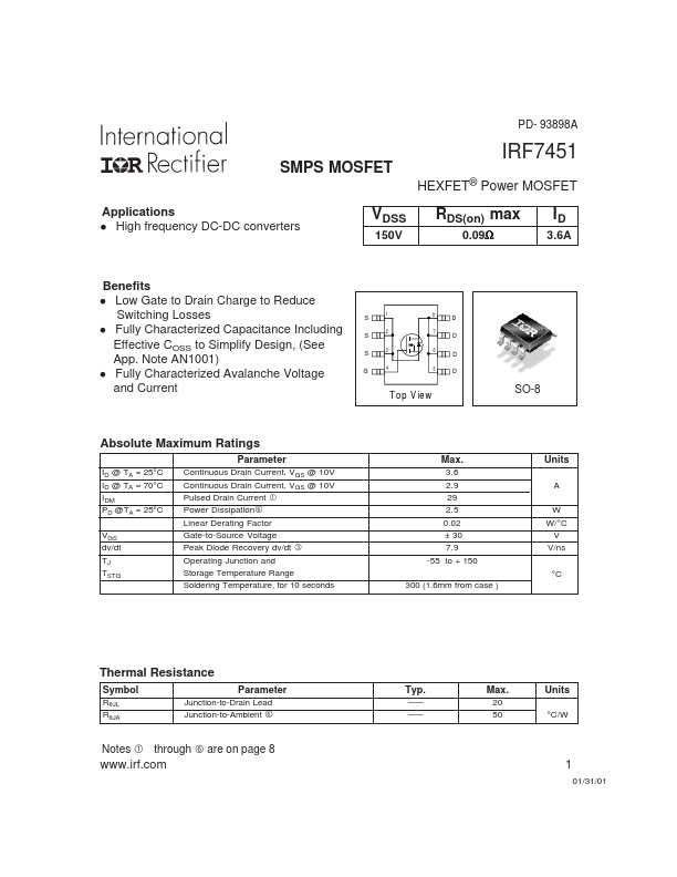
S S S G
1
8 7
A A D D D D
2
3
6
4
5
T o p V ie w
SO-8
Absolute Maximum Ratings
Parameter
ID @ TA = 25°C ID @ TA = 70°C IDM PD @TA = 25°C VGS dv/dt TJ TSTG Continuous Drain Current, VGS @ 10V Continuous Drain Current, VGS @ 10V Pulsed Drain Current Power Dissipation Linear Derating Factor Gate-to-Source
Voltage Peak Diode Recovery dv/dt Operating Junction and Storage Temperature Range Soldering Temperature, for 10 seconds
Max.
3.6 2.9 29 2.5 0.02 ± 30 7.9 -55 to + 150 300 (1.6mm from case )
Units
A W W/°C V V/ns °C
Thermal Resistance
Symbol
RθJL RθJA
Parameter
Junction-to-Drain Lead Junction-to-Ambient
Typ.
––– –––
Max.
20 50
Units
°C/W
Notes through are on page 8
www.irf.com
1
01/31/01
IRF7451
Static @ TJ = 25°C (unless otherwise specified)
Parameter Drain-to-Source Breakdown
Voltage ∆V(BR)DSS/∆TJ Breakdown
Voltage Temp. Coefficient RDS(on) Static Drain-to-Source On-Resistance VGS(th) Gate Threshold
Voltage V(BR)DSS IDSS IGSS Drain-to-Source Leakage Current Gate-to-Source Forward Leakage Gate-to-Source Reverse Leakage Min. 150 ––– ––– 3.0 ––– ––– ––– ––– Typ. ––– 0.19 ––– ––– ––– ––– ––– –––...